Micro Pattern Gas Detectors (MPGD) fabrication processes
|
|
|
- Francine Dickerson
- 6 years ago
- Views:
Transcription
 fabrication processes")


1 Micro Pattern Gas Detectors (MPGD) fabrication processes 1 Silvia Franchino Silvia.franchino@cern.ch Kirchhoff Institute for Physics University of Heidelberg April 2016 HighRR Lecture Week Detector Technology & System Integration session
2 Outline 2 General introduction to MPGD working principles; motivations for their development Examples of MPGDs in HEP Tuning of MPGD parameters ALICE TPC upgrade (GEM) ATLAS Forward Muon Spectrometer (MM) MPGD production process and critical points Large area detector production for HEP. Solutions adopted
3 3 General introduction to MPGD working principles; motivations behind their development
4 Gas Detectors 4 - Cathode Anode Gas volume -
5 Gas Detectors 5 - Cathode Anode Energy loss due to electromagnetic interactions + + Gas volume
6 Gas Detectors 6 - Cathode Anode Energy loss due to electromagnetic interactions + + Gas volume Edrift - -
7 Gas Detectors 7 - Cathode Anode Energy loss due to electromagnetic interactions + + Gas volume Edrift - - Egain


8 Gas Detectors 8 Edrift Egain
9 Ionization chambers Gas Detectors 9 Simplest gas detector No multiplication G=1 Primary electrons collected Applications: Nuclear industry: output proportional to radiation dose (if high enough) Medical radiation measurement Smoke detector (alpha source in air)

10 Gas Detectors 10 Geiger Muller counter Massive photoemission Full detector affected Need high resistor to quench the discharge or gas quenchers Often self-substaining discharges. Need HV cut Very low rate capability (used in dosimetry)
11 Gas Detectors Single wire proportional counter [Rutherford, E. and Geiger, H. (1908)] 11
 Single wire")

 Charpak, G. et al.")


12 Traditional wire gas detectors (1) Single wire proportional counter Drift chamber ATLAS Muons Multi Wire proportional Chambers (MWPC) Charpak, G. et al. (1968) Nobel 1992 ALICE TPC Advantages: Large areas at low prices Flexible geometries Good spatial, energy resolution.. HEP experiments, large areas: muon spectrometer TPC readout LHCb Muons CMS Muons 12
 Slow ion motion Fast gain drop at high fluxes: (<10 khz/cm 2 ) Space charge accumulation, distortion of E field.")
 3) Aging Permanent damage of anode structure after long term exposure to radiation.")
13 Traditional wire gas detectors (2) 13 Advantages: Large areas at low prices Flexible geometries Good spatial, energy resolution.. Limitations: 1) Slow ion motion Fast gain drop at high fluxes: (<10 khz/cm 2 ) Space charge accumulation, distortion of E field. Screening effect for next event 2) Limited multi-track separation Minimum wire distance ~1mm (mechanical instabilities due to electrostatic repulsion) 3) Aging Permanent damage of anode structure after long term exposure to radiation. Formation of solid deposits Gain drops and instabilities Deposited polymers on the wire
14 How to improve gas detectors? 14 Slow ion motion Limited multi-track separation Reduce multiplication region size Faster ion evacuation Higher spatial resolution
15 How to improve gas detectors? 15 Slow ion motion Limited multi-track separation Reduce multiplication region size Faster ion evacuation Higher spatial resolution Micro Pattern Gas Detectors (MPGD) First MPGD: Micro Strip Gas Chamber (MSGC) OED, 1988 Reduction of the size of the detecting cell (~ 100 um) using chemical etching techniques Same working principle as proportional wire chambers o Conversion region (low E drift field) o High E field in well localized regions where multiplication happens
 First MPGD: Micro Strip Gas")
16 How to improve gas detectors? 16 Slow ion motion Limited multi-track separation Reduce multiplication region size Faster ion evacuation Higher spatial resolution Micro Pattern Gas Detectors (MPGD) First MPGD: Micro Strip Gas Chamber (MSGC) OED, 1988 SPARKS DIELECTRIC MATERIAL High field close to both electrodes inter-electrode space is on micron scale, i.e. very sensitive to dust thin electrodes can be seriously damaged Movement of charges when HV is applied Charging up
17 Micro Strip Gas Chamber (MSGC) 17 Pitch > 1 mm mechanical and electrostatic forces Pitch ~ 100 μm lithography technology Advantages of MSGC Small pitch between anode and cathode strips: Fast ion collection Spatial reso ~50μm Two track reso ~500 μm High rate capability ~10 6 Hz/mm A. Oed NIM. A263 (1988) 351. GRENOBLE


18 Micro Strip Gas Chamber (MSGC) 18 Pitch > 1 mm mechanical and electrostatic forces Multi wires Pitch ~ 100 μm lithography technology Micro Strips, different substrates Advantages of MSGC Small pitch between anode and cathode strips: Fast ion collection Spatial reso ~50μm Two track reso ~500 μm High rate capability ~10 6 Hz/mm A. Oed NIM. A263 (1988) 351. GRENOBLE
19 Problems Micro Strip Gas Chamber (MSGC) Efficiency plateau too close to the discharge probability!!! 19 1) Destructive discharges

 Destructive discharges 2) Aging")

20 Problems Micro Strip Gas Chamber (MSGC) Efficiency plateau too close to the discharge probability!!! 20 1) Destructive discharges 2) Aging Thin wire problem 3) Time evolution of the gain: charging up, polarization, movement of charges in the substrate
21 21 Rapid development of many different MPGD structures to improve performances and solve MSGC problems

22 22
23 Today: holes and meshes 23 F. Sauli, NIM. A386(1997)531 I. Giomataris et al., NIM A 376 (1996) 29 GEM (std, Thick, glass, ) Micromegas (bulk, micro bulk, resistive,..)
531 I. Giomataris et al.")
 Micromegas (bulk, micro bulk, resistive,.")

24 Today: holes and meshes 24 F. Sauli, NIM. A386(1997)531 I. Giomataris et al., NIM A 376 (1996) 29 GEM (std, Thick, glass, ) Micromegas (bulk, micro bulk, resistive,..) Aging: OK (no thin wires) Spark protection: multiple amplification stage, resistive electrodes ~100 um gap
25 Gas Electron Multiplier (GEM) Initially developed as a preamplifier stage for an MSGC Sauli, F. (1997) CERN Polliamide (kapton)

 CERN Multiple GEMs high gains (> 10 5")

26 Gas Electron Multiplier (GEM) Initially developed as a preamplifier stage for an MSGC Sauli, F. (1997) CERN Multiple GEMs high gains (> 10 5 ) before discharges, lower voltage for each GEM, spread of the avalanche. GAIN DISCHARGE PROBABILITY Polliamide (kapton)
254 Electrons collected on patterned readout boards.")


27 Triple GEM GEM readout 27 A. Bressan et al, Nucl. Instr. and Meth. A425(1999)254 Electrons collected on patterned readout boards. Typically 2-3 mm diameter electron shower at the readout A fast signal can be detected on the lower GEM electrode for triggering or energy discrimination. Characteristic unique of GEMs: Full decoupling of the charge amplification structure from the charge collection and readout structure. Both structures can be optimized independently. Not only planar shape.
28 GEM principle 28 Garfild simulation,


29 GEM family (R&D ongoing) 29 Thick GEM Diamond GEM Cylindrical GEM Glass GEM Multilayer thick GEM And many others.

 gap, Conversion and amplification regions")
 from pillars.")
30 MICROMEsh Gaseous Structure (Micromegas, MM) (I. Giomataris et al. (1996) SACLAY 30 Parallel plate field Amplification in a thin (100 um) gap, Conversion and amplification regions separated by a fine metallic mesh. Geometrical inefficiency (~1% ) from pillars. High rate applications. Ions created in amplification gap are captured by the mesh


31 Micromegas family (R&D ongoing) Resistive strips MM Embedded resistors MM Ingrid 31 Piggy back resistive MM Microbulk MM And many others. Cylindrical MM
32 MPGD are mostly used in forward regions 32 of HEP experiments were the rate or radiation are too high for normal wire chambers Examples
33 MPGD are mostly used in forward regions 33 of HEP experiments were the rate or radiation are too high for normal wire chambers Every LHC experiments (will) use MPGD Running LS2 Upgrades ( ) LHCb 3 GEM (MS fw) TOTEM 3 GEM (tracker fw) CMS ALICE ATLAS 3 GEM (MS- fw) 4 GEM (TPC) res MM (MS- fw)

")


34 Running LHCb muon trigger (LHC) 34 Requirements of M1 Rate Capability up to 0.5 MHz/cm 2 Station Efficiency 96% in a t 20 ns Low material budget (before calo) radiation hardness GEM choice R&D work done on (RPC much faster but lower rate capability) Two double chambers, triple-gem detectors in OR GEM foils: 20x24 cm 2 Readout: Pad 10x25 mm 2


35 Running TOTEM T2 tracker (LHC) 35 To measure inelastic produced charged particles Very forward region CMS 5.3< η <6.5 Requirements Rate Capability MHz/cm 2 at L= cm -2 s -1 Radiation hardness Efficiency >97% Time resolution < 10 ns Space resolution < 100 μm GEM choice Each side: 20 triple GEM chambers. Readout: strips (tracking) and pads (triggering)


 Large area detector Readout in a")

36 CBM muon (FAIR) 36 Construction in CERN Test beam at GSI Muon detectors requirements High collision rate High track density Radiation resistant (high neutron dose ~10 13 n.eq./sq.cm/year) Large area detector Readout in a self triggered mode For the first two stations, which demand a high rate capability, GEM will be used. TDR approved in 2014


 barrel endcap Sébastien Procureur")
37 CLASS12 FW tracker (JLAB) Study of the nucleon structure with high 12 GeV electron beam at high luminosity 37 Installation in progress - 1st curved Micromegas - 1st use in 5T field - Resistive technology - High rate (30 MHz) barrel endcap Sébastien Procureur CEA-Saclay
38 38 Two examples of detector optimization R&Ds

39 Example on how to tune an MPGD to fulfil the physics requirements ALICE TPC upgrade 39

 TPC as central tracker for many experiments SLAC")
40 TPC Time Projection Chamber 1974, David Nygren 40 C. Brezina Filled with high purity gas Electron amplification with Multi Wire proportional Chamber at the endplates XY coordinate from pad/strips RO plane Z coordinate from drift Critical points: homogeneous drift speed (gas purity, constant E, ion backflow) TPC as central tracker for many experiments SLAC (PEP) LEP (ALEPH, DELPHI) RHIC (STAR) LHC (ALICE) ILC?? (ILD)
 Rate limitation ~3.")
41 TPC ion blocking, gating grid 41 When a trigger appears Primary electrons ALICE TPC I + ~ 1000 times slower than e - Open grid: let electrons in (100 μs) Closed grid: blocks ions created in the avalanche process and not triggered signals from the drift Slow ions Need closed time: 180 μs (time ions takes to drift to the gating grid in Ne based mixtures) Rate limitation ~3.5KHz
.")

 <12% )")
42 ALICE TPC upgrade 42 PHISICS REQUIREMENTS: Increase of rate up to 50 khz Pb-Pb (20 μs). Not possible standard gating (max rate ~3kHz) Need new RO chamber who allow s continuous RO Ion back-flow <1% at G=2000 to keep space charge of TPC at tolerable level. Preserve de/dx resolution of the old chamber for particle ID (Ω/E (Fe55) <12% ) Stable operation at LHC (not redundancy!!) A lot of R&D in the last 3-4 years 4 GEM foils (Approved in 2014). Total area 32.5 m2, up to 112 cm in length
 -- Energy resolution (spectrum Fe55 X ray source) -- Discharge probability (alpha")
.")
43 Detector R&D studies 43 Configuration tried: -- 3 GEMS --4 GEMS -- 4 GEMS different pitch -- 1 MM + 2 GEMs Lab measurement -- Ion BackFlow (vs E fields, rate, gain) -- Energy resolution (spectrum Fe55 X ray source) -- Discharge probability (alpha source, testbeam hadronic showers Many parameters to be tuned: dv each GEM (Gain, E reso, spark probability)+ E transfer fields (Ion Backflow). E reso: collection all primary electrons, good extraction, high transfer field Ion blocking: low transfer field
 <12% Stable operation at LHC (not redundancy!")
44 Detector R&D: E reso, IBF 44 Configuration tried: X 3 GEMS X 4 GEMS 4 GEMS different pitch 1 MM + 2 GEMs Only a small window where requirements are satisfied PHISICS REQUIREMENTS: Ion back-flow <1% at G=2000 Ω/E (Fe55) <12% Stable operation at LHC (not redundancy!!) ALICE Upgrade TPC TDR Addendum to the ALICE Upgrade TPC TDR
 with pion beam + Fe target 45 Discharge")


45 Detector R&D: discharge probability 2 real size prototypes, tested at the SPS (CERN) with pion beam + Fe target 45 Discharge probability MM prototype 2-3 order magnitude higher than 4GEM prototype Final decision for the 4 GEM TPC readout Ion Back Flow Energy resolution Spark rate Ion Back Flow Energy resolution X Spark rate ALICE Upgrade TPC TDR Addendum to the ALICE Upgrade TPC TDR


46 ALICE TPC upgrade 46 ALICE Upgrade TPC TDR Addendum to the ALICE Upgrade TPC TDR


47 How to cope with sparks in micromegas ATLAS new small wheel case 47


 But.")
48 ATLAS NSW upgrade 48 Replacement of current wire detectors to cope with luminosity increase in Run3 Why the Micromegas choice Rate capability 15 khz/cm 2 (L 5 x cm -2 s -1 ) Spatial resolution 100 um, Θtrk< 30 Radiation resistance, no ageing Big surface MPGD The only MPGD that can achieve such dimensions: Micromegas Small Wheels ( η = 1 2.7) But. a long R&D phase to fight against sparks


49 Resistive strips micromegas 49 Inacceptable high spark rate in LHC operation conditions High Voltage drops -> dead times T. Alexopoulos et all, NIM A640 (2011) Sparks still occur but become inoffensive No High Voltage drops Very small current up to G~2*10 4
50 Resistive strips micromegas 50
51 Inclined tracks, spatial resolution 51 The μ-tpc
52 Micromegas with μ-tpc readout 52 Requirements Rate capability 15 khz/cm 2 (L 5 x cm -2 s -1 ) Spatial resolution 100 um, Θtrk< 30 Radiation resistance, no ageing Big surface Spatial resolution rapidly decreases with Θ when charge centroid is used

53 Micromegas with μ-tpc readout 53 Requirements Rate capability 15 khz/cm 2 (L 5 x cm -2 s -1 ) Spatial resolution 100 um, Θtrk< 30 Radiation resistance, no ageing Big surface Spatial resolution rapidly decreases with Θ when charge centroid is used Measuring arrival time of the signal opens a new dimension

54 54 GEM and micromegas Fabrication at CERN


55 MPGD fabrication at CERN Micro Pattern Technology workshop ~20 persons Making PCBs since
56 MPGD fabrication at CERN 56 Base material Micro pattern Photolithography Same technique, equipment as standard printed circuits boards (PCB) fabrication


57 MPGD fabrication at CERN 57 Base material Micro pattern Photolithography Same technique, equipment as standard printed circuits boards (PCB) fabrication + process optimization for MPGD Many years of continuous R&D (e.g. GEM etching, MM pillars, resistive strips) Technology transfer to external industries ongoing (detector fabrication for big experiments)


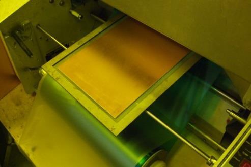
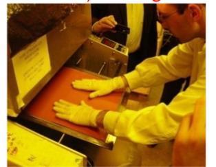
58 Photolithography (1) 58 Chemically etch away the unwanted copper in order to create the wanted image Image/circuit design Base material PCB

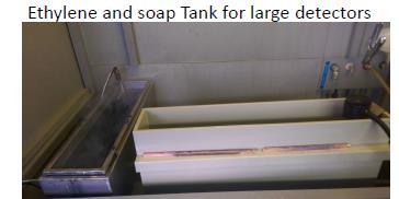
59 Photolithography (2) 59 Design the (complementary) image and print the film Link: A. Teixeira CERN Ph-DT seminar 2015

 Link: A.")
60 Photolithography (3) 60 Embed the base material into a photosensitive material (photoresist) Link: A. Teixeira CERN Ph-DT seminar 2015
 Link: A.")
61 Photolithography (4) 61 Film on top of the photoresist UV exposure Development (sodium carbonate) Link: A. Teixeira CERN Ph-DT seminar 2015
 Link: A.")
62 Photolithography (5) 62 Etching (ferric chloride) Stripping (alcohol) Link: A. Teixeira CERN Ph-DT seminar 2015

 63 CNC drilling")
")


63 Other used processes Photolithography (6) 63 CNC drilling machine (ThickGEM, final cut ) Cleaning/de-chroming baths Press For multilayer circuits. AND MANY MORE.. Kapton etching Micro-etching baths Fial passivation Thin lines RIM thickgems

64 64


 50um copper clad")

65 Production steps 1) Base material GEM std technique: double mask Base material 65 2) Top, Bot mask alignment, UV irradiation 3) Cu etch 4) Kapton etc Examples COMPASS (CERN) TOTEM (CERN) LHCb- μ trigger (CERN) 50um copper clad Polyimide Rolls of 100m x 0.6m Polyimide : APICAL NP or AV One supplier: LSMtron (Korea)
66 1) Base material GEM std technique: double mask Critical point 66 2) Top, Bot mask alignment, UV irradiation 3) Cu etch 4) Kapton etc Film with holes to be aligned under microscope (precision ~ um) Impossible for large foils!!! Max size: 40*40 cm^2 Electric Field and performance strongly related to the hole shape Mask misalignment


67 67 Mesh


68 Standard bulk MM 68 BULK MICROMEGAS Mesh is trapped by pillars. ADVANTAGES Constant amplification gap, maintained by pillars Not warries about readout plane flatness WEAK POINTS Dust: if trapped between mesh and RO during production short, spark, leakage current. Dead detector Bigger the surface, higher probability to trap dust during production pillar mesh RO


69 Making MM pillars 69
70 Photolithography for micro structures, Example of critical points 70 More precision, line width/isolation in the final product thinner the photoresist (30 um stnd, 20 um GEM, 15 um fine lines) and Cu more fragile, more defect sensitive Many parameters to tune: Image accuracy: film print high resolution, film temperature and material (deformation) Vacuum between film and photosensitive material UV irradiation time
71 UV exposure film photoresist Cu dielectric Micro structures, Example of critical points 71 After UV exposure Development. Etching Result Perfect exposure Polymerization of photoresist where film is transparent. Final Cu shape = film image Under exposure Not enough photoresist protection during etching. Breakingdelaminating. Too much etching, irregular shape Over exposure or not perfect vacuum Too much polymerization of photoresist. Bad result
72 Photolithography for micro structures, Example of critical points 72 More precision, line width/isolation in the final product thinner the photoresist (30 um stnd, 20 um GEM, 15 um fine lines) and Cu more fragile, more defect sensitive Many parameters to tune: Image accuracy: film print high resolution, film temperature and material (deformation) Vacuum between film and photosensitive material UV irradiation time Photoresist development (chemical bath concentration, day dependent. To be tuned with development speed) etching time. Same as before raw material thickness disuniformities cleanness during lamination photoresist (cleanroom), well water washing after each chemical process


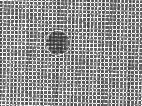
73 (big) Dust in the UV irradiation Not well washed after a chemical bath Micro structures, Example of critical points Dust and cleaning problems Not well developed after UV irradiation Forgotten in a chemical bath during lunchtime 73


74 Technological problem: Not easy to scale in dimensions Large number of large area detectors Micro-precision in macroscopic structures.. 10 cm*10 cm 2 m * 1 m 74
75 75 In the last few years boost on R&D activities to develop large area MPGD Compatible with experiment demands (RD51 project, ATLAS MM, CMS GEM)
 1.6m * 0.")
76 Technological problem: Not easy to scale in dimensions Large area GEM production: Single Mask technique Max size standard technique 40*40 cm 2 Bigger GEM, PRAD (USA) 1.6m * 0.6m 76
 Impossible for large foils!")
77 Double mask 1) Base material GEM new technique: single mask Critical point 77 2) Top, Bot mask alignment, UV irradiation 3) Cu etch 4) Kapton etc Film with holes to be aligned under microscope (precision ~ um) Impossible for large foils!!! Max size: 40*40 cm^2 Electric Field and performance strongly related to the hole shape Mask misalignment
 Top, Bot mask alignment, UV")
 2) Top mask ONLY UV")
 Second kapton etch PRAD (USA) 2m x 60cm due to Base material")
78 Double mask 1) Base material GEM new technique: single mask 1) Same base material 78 Single mask 2) Top, Bot mask alignment, UV irradiation 3) Cu etch 4) Kapton etc Examples CMS muons (CERN) KLOE2 cylindrical GEM (Frascati ITALY) 2) Top mask ONLY UV irradiation 3) Cu top etch 4) Kapton etch 5) Cu bot electro etch 6) Second kapton etch PRAD (USA) 2m x 60cm due to Base material Equipment
 Floating mesh 2) Screen printing resistive strips")
79 Technological problem: Not easy to scale in dimensions ATLAS Micromegas 1) Floating mesh 2) Screen printing resistive strips 79
80 Bulk Mesh embedded in pillars Self supporting Constant amplification gap even if RO plane not perfectly flat Cylindrical detectors Production in clean room mandatory to avoid dust trapping Difficult large area production MM floating mesh (ATLAS) 80


 (ATLAS) Easy to open and clean Lower cost (industrial")
81 Bulk Mesh embedded in pillars Self supporting Constant amplification gap even if RO plane not perfectly flat Cylindrical detectors Production in clean room mandatory to avoid dust trapping Difficult large area production MM floating mesh (ATLAS) Floating mesh Need strong mechanical supports Planarity to be controlled! (to guarantee amplification gap constant) Large sizes (~ 2m) (ATLAS) Easy to open and clean Lower cost (industrial production) 81 Mesh separated from pillars


82 First cosmic measurement of ATLAS big floating mesh MM. Inefficiency.. Life is not so easy.. Electrostatic force push the mesh toward the pillars but If non-flatness RO board over short distance smaller amplification field 82 M. Bianco Stringent requirements of μ-level flatness during production
83 Resistive layers for mass production 83 Photolithography Possibility to go down to 100 um pitch X time consuming for industrial production X If fails, to throw away the full RO board PCB PCB PCB PCB PCB Standard technique used for R&D on first resistive MM prototypes
84 Resistive layers, photolitography Resistive paste manual deposition 84 Optical check and curing


85 Resistive layers, photolitography Resistive paste manual deposition 85 After curing After sandpaper Etch etra Cu Optical check and curing Sandpaper to eliminate extra R paste and reach Cu level Final result


86 Resistive layers, photolitography 86 BIG detectors Feasible but complicated for industrial production, time consuming

87 Resistive layers for mass production 87 Photolithography Possibility to go down to 100 um pitch X time consuming for industrial production X If fails, to throw away the full RO board PCB PCB PCB PCB PCB PCB PCB PCB Screen printing Pitch > 400 um Automatic machine (industry)


88 Resistive layers, screen printing 88


89 Resistive layers for mass production 89 Readout circuit Resistive strips, screen printed on kapton foils Pillar creation

 Carbon paste")


90 Screen printing mass production 90 R&D at CERN, Japan s industry (mass production) Carbon paste deposition After printing Automatically controlled squeegee Drying 170 o A. Ochi s RD51 coll. meeting
 91")


91 Detector cleaning (R&D phase) 91 Opening mechanical structure needed Chemical cleaning baths Going to the CERN workshop for the cleaning Powder capturer in clean room De-mineralised water


92 Questions? 92
93 93


94 94


95 ATLAS NSW 95 Stretching mesh 15 N cm

96 ATLAS quadruplet layout 96
97 Resistive strips MM, rate capability 97 ATLAS rates Gain 5000 Clean signals up to >1 MHz/cm2, but some loss of gain

98 98 P. Iengo (CERN)


99 Kloe2 inner DAPHNE 99 First cilindrical MPGD Installed in cylindrical-gem detectors 41 cm 36 cm 31 cm 26 cm

100 0V +V 100 Protected Top Electrode 0V -Chromic acid Bath Chromic acid : 80 g/l Sulfuric acid H2SO4: 3cc/l room temp Etched electrode +V 0.7 to 1.3V Current control Depending on size From 0.5A (10x10 cm2) up to 6A (1/2 m2)
101 Kapton etching chemistry (60 degrees) 2/3 Etyldiamine (C 2 H 8 N 2 ) g/l Potassium hydroxide (KOH) 1/3 H2O Development Sodium Carbonate

102 102 R. De Oliveira (CERN)

103 103 From H-C Shultz-Coulon lectures
")


104 Large triple-gem assembly (CMS, CBM) 104 New self-stretching technique Electrical test before starting. No sparks, no leakage current Roll to capture dust Readout board 3 GEM foils Drift Detector Base Screws pull And stretch foils


105 ALICE GEM gluing 105 Heidelberg GEM gluing school

106 106

107 107
+ E transfer fields (Ion")
108 Detector R&D studies 108 Many parameters to be tuned: dv each GEM (Gain, E reso, spark probability)+ E transfer fields (Ion Backflow).
arxiv: v1 [physics.ins-det] 2 Oct 2013
![arxiv: v1 [physics.ins-det] 2 Oct 2013](/thumbs/73/68943828.jpg "arxiv: v1 [physics.ins-det] 2 Oct 2013") Preprint typeset in JINST style - HYPER VERSION The Micromegas Project for the ATLAS Upgrade arxiv:1310.0734v1 [physics.ins-det] 2 Oct 2013 G. Iakovidis a,b a National Technical University of Athens Zografou
Preprint typeset in JINST style - HYPER VERSION The Micromegas Project for the ATLAS Upgrade arxiv:1310.0734v1 [physics.ins-det] 2 Oct 2013 G. Iakovidis a,b a National Technical University of Athens Zografou
RECENT DEVELOPMENTS ON MICRO-PATTERN GASEOUS DETECTORS TECHNOLOGY
 RECENT DEVELOPMENTS ON MICRO-PATTERN GASEOUS DETECTORS TECHNOLOGY 0.18 mm CMOS VLSI Ions CMOS high density readout electronics 40 % 60 % Electrons Micromegas GEM THGEM MHSP Ingrid Gabriele Croci (CERN
Micromegas detectors for the upgrade of the ATLAS Muon Spectrometer
 Micromegas detectors for the upgrade of the ATLAS Muon Spectrometer André Zibell Julius-Maximilians-Universität Würzburg On behalf of the ATLAS Muon Collaboration INSTR2014 Conference Novosibirsk, 2014/2/28
Micromegas in a Bulk
 1 Micromegas in a Bulk I. Giomataris 1, R. De Oliveira 2, S. Andriamonje 1, S. Aune 1, G. Charpak 2, P. Colas 1, A. Giganon 1, Ph. Rebourgeard 1, P. Salin 3 1 CEA-DSM/Saclay-France 2 CERN, Geneva, Switzerland
R&D Fast and lightweight EIC integrated tracking system Barrel MicroMegas & Forward Triple-GEM
 1 R&D Fast and lightweight EIC integrated tracking system Barrel MicroMegas & Forward Triple-GEM Franck Sabatie (PI) Matt Posik, Maxence Vandenbroucke, Bernd Surrow (PI) Outline 2 Overview of R&D program
Aging Analysis of Micromegas Detectors for ATLAS New Small Wheel
 Aging Analysis of Micromegas Detectors for ATLAS New Small Wheel Melissa Quinnan August 15, 2015 Supervisor: Michele Bianco Abstract In preparation for the coming High Luminosity Large Hadron Collider
Status Report about the TPC Detector and Module at CEPC
 Status Report about the TPC Detector and Module at CEPC Huirong QI On behalf of CEPC TPC subgroup, IHEP, CAS 2016.01.19, IAS, HK Content Goals and options Some considerations Preliminary simulation Hybrid
GEM detectors activity at the Laboratori Nazionali di Frascati of INFN
 GEM detectors activity at the Laboratori Nazionali di Frascati of INFN M. Alfonsi', G. Bencivenni, P. de Simone, D. Domenici, F. Murtas, M. Pistilli and M. Poli Lener Laboratori Nazionali di Frascati,
Gaseous detectors. 1
 Gaseous detectors Very important class of detectors with many applications charged particle, x- & gamma rays, visible light detection applications in many areas of research, & commercial particle & nuclear
The LHCb Outer Tracker: Production & Ageing studies
 The LHCb Outer Tracker: Production & Ageing studies Kaffeepalaver MPI-K Physikalisches Institut Physikalisches Institut 1 LHC at CERN p-p collisions beam energy 7 TeV 8.6km Four experiments: Atlas, CMS,
Discharge reduction technologies for Micromegas detectors in high hadron flux environments
 Journal of Instrumentation OPEN ACCESS Discharge reduction technologies for Micromegas detectors in high hadron flux environments To cite this article: M Vandenbroucke View the article online for updates
Aging measurements on triple-gem detectors operated with CF 4 based gas mixtures
 IEEE, Roma, October 2004 Aging measurements on triple-gem detectors operated with CF 4 based gas mixtures M. Alfonsi 1, G. Bencivenni 1, W. Bonivento 2,A.Cardini 2, P. de Simone 1, F.Murtas 1, D. Pinci
R&D of GEM detector high rate for CBM Experiment at FAIR Muon Chamber R&D in India
 R&D of GEM detector high rate for CBM Experiment at FAIR Muon Chamber R&D in India Pradeep Ghosh Facility for Antiproton and Ion Research (FAIR) in Europe, Darmstadt - Germany ERICE, ISSP 2017 CBM @ FAIR
A Triple GEM Detector for the central Region of Muon Station 1
 A Triple GEM Detector for the central Region of Muon Station 1 M. Alfonsi 1, G. Bencivenni 1, W. Bonivento 2, A.Cardini 2, C. Deplano 2, P. de Simone 1, F. Murtas 1, D. Pinci 3, M. Poli-Lener 1, D. Raspino
New spark-protected GEMlike detectors with resistive electrodes
 New spark-protected GEMlike detectors with resistive electrodes V. Peskov Behalf of ALICE HMPID, ICARUS research group and TS/DEM/PMT Workshop CERN The talk today will be about breakthrough in developments
IFIN-HH, Hadron Physics Department infrastructure for ALICE TPC upgrade
 Hadron Physics Department IFIN-HH, Hadron Physics Department infrastructure for ALICE TPC upgrade M. Petris, M. Petrovici, V. Aprodu, D. Bartos, A. Bercuci, Gh. Caragheorgheopol, V. Catanescu, V. Duta,
THE muon system of the Compact Muon Solenoid (CMS)
") This work has been submitted to the IEEE Nucl. Sci. Symp. 2010 for publication in the conference record. Copyright may be transferred without notice, after which this version may no longer be available.
This work has been submitted to the IEEE Nucl. Sci. Symp. 2010 for publication in the conference record. Copyright may be transferred without notice, after which this version may no longer be available.
February 12, PHY357 Lecture 11. Experimental Methods. Accelerators. Particle Interactions. Particle Detectors. Full experiment (eg.
 PHY357 Lecture 11 Experimental Methods Accelerators Particle Interactions Particle Detectors Full experiment (eg. ATLAS) Introduction! Several different general classes of particle detectors (sensors)!
Aging tests with GEM-MSGCs
 1 Aging tests with GEM-MSGCs M. Hildebrandt a, a Physik-Institut Universität Zürich, CH - 8057 Zürich, Switzerland The Inner Tracker of the HERA-B experiment at the Deutsches Elektronen-Synchrotron (DESY)
arxiv: v1 [physics.ins-det] 10 May 2017
![arxiv: v1 [physics.ins-det] 10 May 2017](/thumbs/95/126094881.jpg "arxiv: v1 [physics.ins-det] 10 May 2017") Measurement of basic characteristics and gain uniformity of a triple GEM detector Rajendra Nath Patra a, Rama N. Singaraju a, Saikat Biswas b, Zubayer Ahammed a, Tapan K. Nayak a,c, Yogendra P. Viyogi
Measurement of basic characteristics and gain uniformity of a triple GEM detector Rajendra Nath Patra a, Rama N. Singaraju a, Saikat Biswas b, Zubayer Ahammed a, Tapan K. Nayak a,c, Yogendra P. Viyogi
PERSPECTIVES OF MICRO-PATTERN GASEOUS DETECTOR TECHNOLOGIES FOR FUTURE PHYSICS PROJECTS
 PERSPECTIVES OF MICRO-PATTERN GASEOUS DETECTOR TECHNOLOGIES FOR FUTURE PHYSICS PROJECTS M. Titov CEA Saclay, IRFU/SPP, Gif sur Yvette, France A centenary after the invention of the basic principle of gas
PERSPECTIVES OF MICRO-PATTERN GASEOUS DETECTOR TECHNOLOGIES FOR FUTURE PHYSICS PROJECTS 1
 arxiv: 1308.3047 M. Titov. Perspectives of MPGD Technologies for Future Physics Projects 1 PERSPECTIVES OF MICRO-PATTERN GASEOUS DETECTOR TECHNOLOGIES FOR FUTURE PHYSICS PROJECTS 1 Maxim Titov CEA Saclay,
Experimental Particle Physics PHYS6011 Joel Goldstein, RAL
 Experimental Particle Physics PHYS6011 Joel Goldstein, RAL 1. Introduction & Accelerators 2. Particle Interactions and Detectors (1/2) 3. Collider Experiments 4. Data Analysis Charged Particle Detectors
Antoine Drouart DSM/DAPNIA/SPhN. Köln, 5 th of December,
 Köln, 5 th of December, 2007 1 Basic CATS/BTD mechanics Köln, 5 th of December, 2007 2 Beam Tracking Today -Detector able to cope with a few 10 5 pps -Spatial resolution (FWHM) : 0.7mm -Time resolution
New pixelized Micromegas detector for the COMPASS experiment
 New pixelized Micromegas detector for the COMPASS experiment Damien Neyret a1, Marc Anfreville a, Yann Bedfer a, Etienne Burtin a, Nicole d'hose a, Arnaud Giganon a, Bernhard Ketzer b, Igor Konorov b,
TPC BASED IMP. Limin Duan, Gas Detector Group. Institute of Modern Physics, CAS TPC tracker detector technology mini-workshop
 TPC BASED GEM @ IMP Limin Duan, Gas Detector Group Institute of Modern Physics, CAS 2016.09.01 Beijing,IHEP TPC tracker detector technology mini-workshop Outline 2 Gas detector group GEM-readout TPC a
A Fast Multi-GEM based Detector for High-Rate Charged-Particle Triggering
 A Fast Multi-GEM based Detector for High-Rate Charged-Particle Triggering G. Bencivenni, W. Bonivento, A. Cardini, C. Deplano, P. De Simone, G. Felici, D. Marras, F. Murtas, D. Pinci, M. Poli-Lener and
A GEM-based detector for detection and imaging sparks and flames G. Volpe 1 and V. Peskov 2. Abstract
 A GEM-based detector for detection and imaging sparks and flames G. Volpe 1 and V. Peskov 2 1 Dipartimento Interateneo di Fisica \M. Merlin" and Sezione INFN, Bari, Italy 2 CERN and Institute for Chemical
Commissioning of the Silicon Drift Detector of the ALICE experiment at the LHC
 Silicon Drift Detector of ALICE Commissioning of the Silicon Drift Detector of the ALICE experiment at the LHC Emanuele Biolcati for ALICE collaboration Dipartimento di Fisica dell Università di Torino
LCTPC Setup at the DESY Testbeam. AWLC 14, Fermilab , R. Diener, DESY
 Setup at the DESY AWLC 14, Fermilab 14.05.2014, R. Diener, DESY Page 1 DESY II facility offers 3 beam lines with 1-6 GeV electrons Infrastructure DESY II / Area 24/1 telescopes Solenoid and Dipole magnet
Texas active target (TexAT) detector part 1: Design and construction progress
 detector part 1: Design and construction progress") Texas active target (TexAT) detector part 1: Design and construction progress E. Koshchiy, G.V. Rogachev, E. Uberseder, and E. Pollacco 1 1 IRFU, CEA Saclay,Gif-Sur-Ivette, France Construction of a general
Texas active target (TexAT) detector part 1: Design and construction progress E. Koshchiy, G.V. Rogachev, E. Uberseder, and E. Pollacco 1 1 IRFU, CEA Saclay,Gif-Sur-Ivette, France Construction of a general
2008 JINST 3 S The CMS experiment at the CERN LHC THE CERN LARGE HADRON COLLIDER: ACCELERATOR AND EXPERIMENTS.
 PUBLISHED BY INSTITUTE OF PHYSICS PUBLISHING AND SISSA RECEIVED: January 9, 2008 ACCEPTED: May 18, 2008 PUBLISHED: August 14, 2008 THE CERN LARGE HADRON COLLIDER: ACCELERATOR AND EXPERIMENTS The CMS experiment
Application of gaseous detectors for full-field EDXRF imaging of works of art
 Application of gaseous detectors for full-field EDXRF imaging of works of art Pawel Wrobel Faculty of Physics and Applied Computer Science AGH UST, Krakow, Poland Joint ICTP-IAEA Workshop on Advances in
Highlights and Visions of LC Detectors
 Claude Vallée CPPM/DESY Highlights and Visions of LC Detectors LC detector specifications Subdetector technologies Global detector concepts Towards detector Collaborations Disclaimer: not a technical expert
The TOTEM Detector at LHC
 The TOTEM Detector at LHC CMS TOTEM Gennaro Ruggiero /CERN-PH on the behalf of the TOTEM Collaboration TOTEM Collaboration: Bari, Budapest, Case Western Reserve, CERN, Genova, Helsinki, Penn State, Pisa/Siena,
Particle Detectors. Summer Student Lectures 2007 Werner Riegler, CERN, History of Instrumentation History of Particle Physics
 Particle Detectors Summer Student Lectures 2007 Werner Riegler, CERN, werner.riegler@cern.ch History of Instrumentation History of Particle Physics The Real World of Particles Interaction of Particles
Technical Manual Ionisation Chamber MUSIC80
 Technical Manual Ionisation Chamber MUSIC80 Entwicklungsbüro Dr. R. Schneider Lärchenstraße 9 85640 Putzbrunn Tel: 089 608 533 71 Fax: 089 608 533 72 E-Mail: robert@schneider.net Entwicklungsbüro Andreas
Today s Outline - September 12, C. Segre (IIT) PHYS Fall 2016 September 12, / 21
 PHYS Fall 2016 September 12, / 21") Today s Outline - September 12, 2016 C. Segre (IIT) PHYS 570 - Fall 2016 September 12, 2016 1 / 21 Today s Outline - September 12, 2016 Detectors C. Segre (IIT) PHYS 570 - Fall 2016 September 12, 2016
Today s Outline - September 12, 2016 C. Segre (IIT) PHYS 570 - Fall 2016 September 12, 2016 1 / 21 Today s Outline - September 12, 2016 Detectors C. Segre (IIT) PHYS 570 - Fall 2016 September 12, 2016
The Compact Muon Solenoid Experiment. Conference Report. Mailing address: CMS CERN, CH-1211 GENEVA 23, Switzerland
 Available on CMS information server CMS CR -2016/298 The Compact Muon Solenoid Experiment Conference Report Mailing address: CMS CERN, CH-1211 GENEVA 23, Switzerland 28 October 2016 (v2, 25 November 2016)
DR.RUPNATHJI( DR.RUPAK NATH )
") Abstract In the last decade, several new imaging gaseous detectors, called micro-pattern gaseous detectors, have been conceived and rapidly developed. In this paper, the most popular designs of these detectors
Abstract In the last decade, several new imaging gaseous detectors, called micro-pattern gaseous detectors, have been conceived and rapidly developed. In this paper, the most popular designs of these detectors
System Test of the ATLAS Muon Spectrometer in the H8 Beam at the CERN SPS
 TAUP 2780-04 15 Nov 2004 System Test of the ATLAS Muon Spectrometer in the H8 Beam at the CERN SPS Erez Etzion On behalf of the ATLAS Muon Collaboration Abstract--An extensive system test of the ATLAS
ATLAS Beam Abort System Using CVD Diamond Sensors
 ATLAS Beam Abort System Using CVD Diamond Sensors 1. Signal collection in CVD diamond 2. The state of the art in Diamond sensors 3. Diamond monitors at e + e B factories 4. Application to LHC 5. Proposal
I Seminario Nazionale Rivelatori Innovativi
 I Seminario Nazionale Rivelatori Innovativi Monday 30 November 2009 - Friday 04 December 2009 INFN - Laboratori Nazionali di Frascati Programme I Seminario Nazionale Rivelatori Innovativi / Programme Wednesday
Aging Tests of of Full Scale CMS Cathode Strip Muon Chambers
 Aging Phenomena in Gaseous Detectors Aging Tests Full Scale CMS Cathode Strip Muon Chambers CMS Endcap Muon Collaboration Oleg Prokiev Fermilab, Batavia, IL, IL, USA USA Oleg Prokiev Aging Phenomena in
Tracking Detectors 2 silicon for HEP
 Tracking Detectors 2 silicon for HEP Prof. Peter R Hobson C.Phys M.Inst.P. Department of Electronic and Computer Engineering Brunel University London Peter.Hobson@brunel.ac.uk Dr Revised C Da December
A Beam radiation monitor for the SVT based on CVD diamond sensors!
 A Beam radiation monitor for the SVT based on CVD diamond sensors! R. Cardarelli and Anna Di Ciaccio! INFN and Tor University!! Outline! Short review of CVD diamond sensors employed as beam monitoring
Status Report on the Upgrade of the CMS muon system with triple-gem detectors
 Status Report on the Upgrade of the CMS muon system with triple-gem detectors Gilles De Lentdecker Université Libre de Bruxelles (ULB) Brussels, Belgium On behalf of the CMS Collaboration Triple-GEM detectors
Status of the LHCb Detector. LHCC Open Session CERN, 27 November 2002 Werner Witzeling on behalf of the LHCb Collaboration
 Status of the LHCb Detector LHCC Open Session CERN, 27 November 2002 Werner Witzeling on behalf of the LHCb Collaboration Content Vertex Locator Magnet Outer Tracker RICH2 Calorimeters Muon Detector Online
STATUS OF THE LHC EXPERIMENTS.
 STATUS OF THE LHC EXPERIMENTS. Mario Calvetti Chairman of the LHC Committee INFN and University of Florence calvetti@fi.infn.it Abstract A brief description of the status of the preparation of the large
The ATLAS detector: status of the construction and installation a year before the first p-p collisions at the LHC Collider
 The ATLAS detector: status of the construction and installation a year before the first p-p collisions at the LHC Collider A. Di Ciaccio Università di Roma Tor Vergata and INFN, Roma, Italy On Behalf of
Detectors Plans for LS1
 Detectors Plans for LS1 Chamonix, February 8 th, 2012 M.Nessi + A.Ball, R.Linder, W.Riegler 1 Our present understanding of LS1 Detectors access: 17-24 th November 2012 till mid July 2014 Delivered Luminosity
multi-purpose detector to search for Higgs and new physics
 Status Report on GR-BIS ATLAS Chambers Theodoros Alexopoulos on behalf of the Greek ATLAS Team 2005 Workshop on Recent Advances in Particle Physics and Cosmology ARISTOTLE UNIVERSITY OF THESSALONIKI 21-24
INFN Rome Silicon Microstrip Detector for SBS F. De Persio S. Kiprich - F. Meddi G.M. Urciuoli
 INFN Rome Silicon Microstrip Detector for SBS F. De Persio S. Kiprich - F. Meddi G.M. Urciuoli 1 Summary 1) About us: Presentation of the JLAB12 INFN Roma group. 2) Silicon Detector Advantages on SBS:
CMS, In Brief. Bill Gabella Vanderbilt Quarknet session, July 20, 2015 (disgracefully borrowing from Will Johns)
") CMS, In Brief Bill Gabella Vanderbilt Quarknet session, July 20, 2015 (disgracefully borrowing from Will Johns) CMS, status CMS is up and running after Long Shutdown One (LS1). Yes, there will be an LS2
CMS, In Brief Bill Gabella Vanderbilt Quarknet session, July 20, 2015 (disgracefully borrowing from Will Johns) CMS, status CMS is up and running after Long Shutdown One (LS1). Yes, there will be an LS2
Drift Chamber construction for ATLAS*
 Drift Chamber construction for ATLAS* D. Sampsonidis for the ATLAS group of Thessaloniki Aristotle University of Thessaloniki CERN and the Technology Transfer in Greece Amphitheatre N.C.S.R. DEMOKRITOS,
Institute for Scientific and Technological Research
 ITC-irst Institute for Scientific and Technological Research Trento Italy http://www.itc.it/ ITC-irst ITC-irst is part of Istituto Trentino di Cultura (ITC) Founded in 1976 Dimensions: Full time researchers:
Status of the PRad Experiment (E )
") Status of the PRad Experiment (E12-11-106) Jefferson Lab User Group Meeting 2016 Chao Peng Duke University For the PRad Collaboration Outline PRad Physics Motivation Experimental Setup Current Status Preliminary
Status of the PRad Experiment (E12-11-106) Jefferson Lab User Group Meeting 2016 Chao Peng Duke University For the PRad Collaboration Outline PRad Physics Motivation Experimental Setup Current Status Preliminary
AIDA Advanced European Infrastructures for Detectors at Accelerators. Presentation. LumiCal alignment system, status report
 AIDA-SLIDE-2015-016 AIDA Advanced European Infrastructures for Detectors at Accelerators Presentation LumiCal alignment system, status report Kielar, E (IFJPAN) et al 12 November 2012 The research leading
Development of the CMS Phase-1 Pixel Online Monitoring System and the Evolution of Pixel Leakage Current
 Development of the CMS Phase-1 Pixel Online Monitoring System and the Evolution of Pixel Leakage Current Fengwangdong Zhang On behalf of CMS Pixel Collaboration The 9th International Workshop on Semiconductor
Customized MCPs for Analytical Instruments. An MCP for every application
 Customized MCPs for Analytical Instruments An MCP for every application What are Microchannel Plates? (MCPs) Microchannel plates (MCPs) are solid state detectors consisting of parallel arrays of tiny single
SILICON SENSOR ACTIVITIES AT SINTEF MINALAB. Marco Povoli, Angela Kok, Ozhan Koybasi
 SILICON SENSOR ACTIVITIES AT SINTEF MINALAB Marco Povoli, Angela Kok, Ozhan Koybasi Outline 1. SINTEF MiNaLab 2. Silicon radiation detector history Pad, strip, pixel and silicon drift detectors 3. Overview
Compact Muon Solenoid Detector (CMS) & The Token Bit Manager (TBM) Alex Armstrong & Wyatt Behn Mentor: Dr. Andrew Ivanov
 & The Token Bit Manager (TBM) Alex Armstrong & Wyatt Behn Mentor: Dr. Andrew Ivanov") Compact Muon Solenoid Detector (CMS) & The Token Bit Manager (TBM) Alex Armstrong & Wyatt Behn Mentor: Dr. Andrew Ivanov CERN Conseil Européen pour la Recherche Nucléaire (European Council for Nuclear
Compact Muon Solenoid Detector (CMS) & The Token Bit Manager (TBM) Alex Armstrong & Wyatt Behn Mentor: Dr. Andrew Ivanov CERN Conseil Européen pour la Recherche Nucléaire (European Council for Nuclear
PoS(ICHEP2012)516. The status of the CMS pixel upgrade detector
516. The status of the CMS pixel upgrade detector") University of California Riverside E-mail: Ferdinando.Giordano@cern.ch The present CMS pixel detector was designed for a maximum luminosity of 34 cm s. Following the Phase upgrade of the LHC, the peak
University of California Riverside E-mail: Ferdinando.Giordano@cern.ch The present CMS pixel detector was designed for a maximum luminosity of 34 cm s. Following the Phase upgrade of the LHC, the peak
The Compact Muon Solenoid Experiment. Conference Report. Mailing address: CMS CERN, CH-1211 GENEVA 23, Switzerland. Status of CMS Commissioning
 Available on CMS information server CMS CR-2008/045 The Compact Muon Solenoid Experiment Conference Report Mailing address: CMS CERN, CH-1211 GENEVA 23, Switzerland 21 July 2008 Status of CMS Commissioning
Solid State Detectors. T. Bowcock
 Solid State Detectors T. Bowcock Schedule 1 Time and Position Sensors 2 Principles of Operation of Solid State Detectors 3 Techniques for High Performance Operation 4 Environmental Design 5 Measurement
Expected needs in Electronics for the CERN Experiments. 5 October 2015
 Expected needs in Electronics for the CERN Experiments 5 October 2015 Philippe.Farthouat@cern.ch 2 The LHC Experiments 3 ATLAS Detector 4 CMS Detector 5 Collaborations Last generation of HEP detectors
CMS inner detector: the Run 1 to Run 2 transition and first experience of Run 2
 CMS inner detector: the Run 1 to Run 2 transition and first experience of Run 2 Physik-Institut, Universität Zürich, Winterthurerstrasse 190, 8057 Zurich, Switzerland E-mail: clemens.lange@cern.ch The
The Technical Infrastructure Group supplies experimental activities at NBI with technical
 TECHNICAL INFRASTRUCTURE Staff: Leif Antvorskov John Engelhardt Fin Hansen Erik Grønbæk Jakobsen Niels Lindegaard Erik Kaimer Olsen Bjørn Rasmussen Jette Sørensen Henrik Bertelsen Finn Ferrall Jimmy Cali
HOT BAR REFLOW SOLDERING FUNDAMENTALS by Amada Miyachi Europe A high quality Selective Soldering Technology
 HOT BAR REFLOW SOLDERING FUNDAMENTALS by Amada Miyachi Europe A high quality Selective Soldering Technology Content 1. Hot Bar Reflow Soldering Introduction 2. Application Range 3. Process Descriptions
OPERATION MANUAL Model 800 Nanoimprint Controller
 OPERATION MANUAL Model 800 Nanoimprint Controller 685 RIVER OAKS PARKWAY SAN JOSE, CA 95134 www.oainet.com sales@oainet.com 408/232-0600 0420-757-01, Rev. B 02/17/09 OAI Model 800 Nanolithosolution Nanoimprint
The SLAC Detector R&D Program
 The SLAC Detector R&D Program David MacFarlane DOE Site Visit September 14, 2010 Detector R&D Program Page 1 Overview of detector R&D program KA15 detector R&D program includes Core engineering and generic
HiRadMat facility at the CERN SPS
 High-Radiation to Materials HiRadMat facility at the CERN SPS More information at http://cern.ch/hiradmat Adrian Fabich IWSMT-12, Bregenz, 20 th October 2014 Motivation of HiRadMat Dedicated facility for
When Precision is not good enough
 When Precision is not good enough Andrew Kelley XACT PCB Ltd North Shields, UK Abstract As PCB designs become ever more complex with more sequential build up layers, tighter annular ring designs and broader
The Compact Muon Solenoid Experiment. Conference Report. Mailing address: CMS CERN, CH-1211 GENEVA 23, Switzerland
 Available on CMS information server CMS CR -2017/432 The Compact Muon Solenoid Experiment Conference Report Mailing address: CMS CERN, CH-1211 GENEVA 23, Switzerland 23 November 2017 (v3, 14 December 2017)
UV-Ozone Technology and Applications
 UV-Ozone Technology and Applications Introducing SAMCO Your Global Partner in Progress Over the last 30 Years SAMCO has provided Over 3,200 Thin Film Solutions to our Global Partners in 23 Countries The
Understanding Etched Foil Flexible Heaters
 Understanding Etched Foil Flexible Heaters J. Stopperan, Business Development All Flex Flexible Circuits and Heaters May 4, 2012 Flexible heaters is a product family that generically describes thin and
Bonn testbeam, QUAD development
 Bonn testbeam, QUAD development NIKHEF Nikhef/Bonn LepCol meeting May 22, 2017 Monday June 5 Time schedule GridPix testbeam Bonn Fred and Kevin arriving at Bonn with equipment Unloading equipment in institute
ATLAS Diamond Beam Conditions Monitor
 Vertex 2008 17th International Workshop on Vertex Detectors 27th July 1st August 2008, Üto, Stockholm, Sweden ATLAS Diamond Beam Conditions Monitor Irena Dolenc on behalf of the ATLAS BCM Collaboration
LECTURE 11. Dr. Teresa D. Golden University of North Texas Department of Chemistry
 LECTURE 11 Dr. Teresa D. Golden University of North Texas Department of Chemistry C. Detectors Properties of Detectors -quantum counting efficiency -linearity -energy proportionality -resolution C. Detectors
Diamond Detectors Ltd. Fabrication and Packaging Capabilities. Kevin Oliver
 Diamond Detectors Ltd Fabrication and Packaging Capabilities Kevin Oliver Presentation Contents Brief Background. DDL road map to expand our capabilities further Diamond detector application examples.
50(394) IEC. ore content meter ore sorting equipment overvoltage (of a Geiger-Müller county tube)...
 IEC. ore content meter ore sorting equipment overvoltage (of a Geiger-Müller county tube)...") INDEX A (absorbed) dose ratemeter... 394-11-17 absorption band (of a scintillator)... 394-18-08 acceptance test... 394-20-09 accident monitor... 394-12-27 activator... 394-10-08 actuated equipment... 394-14-05
INDEX A (absorbed) dose ratemeter... 394-11-17 absorption band (of a scintillator)... 394-18-08 acceptance test... 394-20-09 accident monitor... 394-12-27 activator... 394-10-08 actuated equipment... 394-14-05
MD456: Monitoring of abort gap population with diamond particle detectors at the BGI in IP 4
 CERN-ACC-NOTE-016-0011 February 15, 016 oliver.stein@cern.ch MD56: Monitoring of abort gap population with diamond particle detectors at the BGI in IP Oliver Stein / TE-MPE Keywords: abort gap, beam gas
ATLAS Pixel Upgrade for HL-LHC
 ATLAS Pixel Upgrade for HL-LHC Elisabeth Petit on behalf of the LPSC and LAPP teams Enigmass general meeting 9th of December 2016 1 The teams Physicists: P. Barroca, S. Jézéquel, R. Lafaye, J. Levêque,
SILICON DRIFT DETECTORS
 SILICON DRIFT DETECTORS PRODUCT BROCHURE 2 JUNE 2018 About PNDetector PNDetector is well-known as a manufacturer of high performance radiation detectors for microanalysis, quality assurance and material
LHCb Rich Detectors Control and High Voltage Systems
 LHCb Rich Detectors Control and High Voltage Systems Mario Sannino On behalf of LHCb RICH Group Rich 2007 Trieste 19.10.2007 1 Rich 2007 Trieste 19.10.2007 LHCb Rich Detectors Control and High Voltage
Perspectives and requirements of new Particle Detectors for future applications.
 Lecture 3 Perspectives and requirements of new Particle Detectors for future applications. V. Peskov, CERN 1 Detector s requirements are driven by the applications 2 What new applications of new gaseous
Minco SmartHeat SLT Self-Limiting Thin-Film Heater Technology
 Minco SmartHeat SLT Self-Limiting Thin-Film Heater Technology Brian Lindgren, Design Engineer, Minco 7300 Commerce Lane North Minneapolis, MN 55432 Tel 763.571.3121 Fax 763.571.0927 minco.com 2 Table of
SYNCHROTRON RADIATION ABSORPTION AND VACUUM ISSUES IN THE IR*
 SYNCHROTRON RADIATION ABSORPTION AND VACUUM ISSUES IN THE IR* J. T. Seeman, SLAC, Menlo Park, CA 94025 USA Abstract The PEP-II B-Factory (3.1 GeV e+ x 9.0 GeV e-) at SLAC operated from 1999 to 2008, delivering
ESTB Proposal from the Stony Brook University: Test of a RICH-Prototype Based on CsI-GEMs
 ESTB Proposal from the Stony Brook University: Test of a RICH-Prototype Based on CsI-GEMs K. Dehmelt, N. Feege, H. Ge, T. K. Hemmick, T. Videbaek, S. Yalçin, S. Zajac Department of Physics and Astronomy
CO 2 COOLING FOR THE LHCB-VELO EXPERIMENT AT CERN.
 GL2008 8 th IIF/IIR Gustav Lorentzen Conference on Natural Working Fluids 7-10 September 2008 Copenhagen, Denmark Paper number: xxx CO 2 COOLING FOR THE LHCB-VELO EXPERIMENT AT CERN. B. Verlaat*, A. Van
Diamond as potential CryoBLM for the LHC All results are preliminary
 Diamond as potential CryoBLM for the LHC All results are preliminary With Marcin Bartosik, Bernd Dehning, Mariusz Sapinski and acknowledgments Christoph Kurfuerst for CryoBLM Team BE-BI-BL CERN Outline
ELEMENT SIX NEWS. Kevin Oliver Business Development Manager NoRDHia August Making Diamond Work for You
 ELEMENT SIX NEWS Kevin Oliver Business Development Manager (Kevin.Oliver@e6.com) NoRDHia August 2006 Making Diamond Work for You E6-General NEWS NEW Diamond Device Electronics Expect an announcement on
THE THERMOSIPHON COOLING SYSTEM OF THE ATLAS EXPERIMENT AT THE CERN LARGE HADRON COLLIDER
 THE THERMOSIPHON COOLING SYSTEM OF THE ATLAS EXPERIMENT AT THE CERN LARGE HADRON COLLIDER M. Battistin, S. Berry, A. Bitadze, P. Bonneau, J. Botelho-Direito, G. Boyd, F.Corbaz, O. Crespo-Lopez, E.Da Riva,
Semiconductor Radiation Detectors
 Gerhard Lutz Semiconductor Radiation Detectors Device Physics With 167 Figures and 11 Tables Contents 1. Introduction 1 Part I: Semiconductor Physics 5 2. Semiconductors 7 2.1 Crystal Structure 7 2.2 Energy
MC-PAD FP7 Marie Curie Initial Training Network on Particle Detectors. Christian J. Schmidt, 4 th NoRHDia Workshop
 MC-PAD FP7 Marie Curie Initial Training Network on Particle Detectors Christian J. Schmidt, 4 th NoRHDia Workshop GSI, Darmstadt, June 8 th -10 th 2008 MC-Pad, Marie Curie Initial Training Network within
ND280 Construction Status Report
 ND280 Construction Status Report Overview Since the last collaboration meeting, the ND280 detector project has undergone a huge transition: January 2009: most efforts focussed at home institutions July
Diamond Windows & MCP Detectors for Synchrotron Applications
 Torr Scientific Ltd. Specialists in UHV, Optical and X-ray Components Diamond Windows & MCP Detectors for Synchrotron Applications www.torrscientific.co.uk Torr Scientific Ltd. Specialists in UHV, Optical
Photolithography SOPs
 Photolithography SOPs The standard operation procedures (SOPs) provided here are to apply the Keck Facility to do microfabrication. Detailed SOPs for each individual photoresist such as the spin coat speed
Mechanical Concept of the TESLA Detector
 Mechanical Concept of the TESLA Detector Klaus Sinram Snowmass August 2005 Ties Behnke, FLC Franz Czempik, ZMEA1 Peter Hassler, ZM1 Helmut Hirsemann, ZMEA1 Jan Kuhlmann, ZMEA1 Cornelius Martens, ZM1 Norbert
Detector Configurations for the MAJORANA Demonstrator
 Detector Configurations for the MAJORANA Demonstrator Lawrence Livermore National Laboratory UC Berkeley 1 How to determine the best configuration for Majorana? Define a metric reflecting the performance