Single Wafer Thin Film Processing Systems
|
|
|
- Griffin Cole
- 5 years ago
- Views:
Transcription


1 Single Wafer Thin Film Processing Systems 3019 Alvin Devane Blvd., Suite 300, Austin, Texas Ph ; Fax
2
3 Single Wafer Thin Film Processing Systems Deposition E-Beam, PECVD, PLD, DLC, DC & RF Sputtering, Ion Beam Sputtering, Thermal Evaporation Etching RIE, DRIE, ICP, Ion Beam Milling & Etching, Plasma, Wet Growth PE-ALD, PA-MOCVD, CNT, DLC, Diamond, Graphene Surface Treatment Ion Beam, PIII, Plasma Cleaning - Dry: Ion Beam, Plasma - Wet: Megasonic, Brush, Piranha, O 3 DIW Other Space Simulation Systems, Heated Platens, Plasma Sources, Ashing, Resist Stripping (Dry & Wet)
 for Semiconductor, Photovoltaic and MEMS applications.")
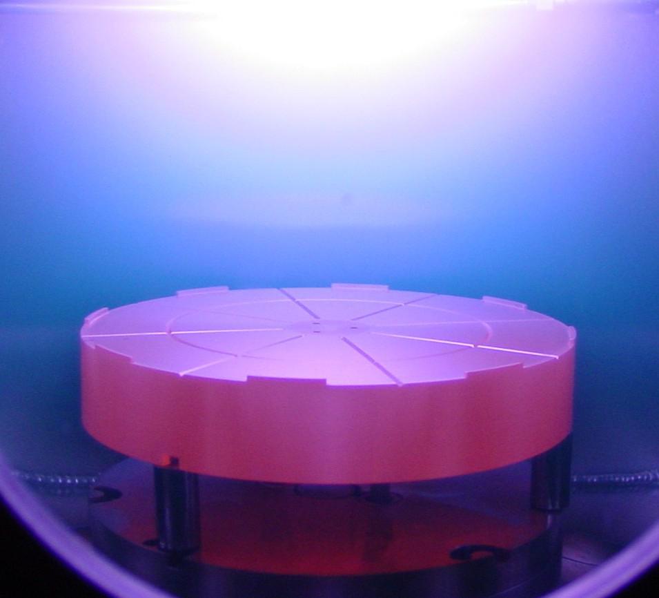
4 Plasma Enhanced Atomic Layer Deposition Systems The NLD-4000 is a stand alone PC controlled ALD system which is fully automated and safety-interlocked having capabilities to deposit oxides and nitrides (e.g. AlN, GaN, TaN, TiN, Al 2 O 3, AlN, TiN, ZrO 2, LaO 2, HfO 2 ) for Semiconductor, Photovoltaic and MEMS applications. It has a 13" aluminum chamber with heated walls and a pneumatically lifted top for easy access. The system features an onboard glovebox which can accommodate an array of up to seven heated or cooled 50cc cylinders for precursors and reactants incorporating fast-pulse delivery valves for pulsed gas input. Unreacted precursors can be captured with a heated filter on the chamber exhaust port. Recipes, temperature setpoints, gas flows, pumpdown and vent cycles, and the flushing of delivery lines are all controlled automatically via LabVIEW software. Options include automatic load/unload (without changing system footprint), Planar ICP source with remote plasma for Plasma Enhanced ALD (Planar ICP geometry maintains a small reaction chamber volume for faster cycle times), and turbomolecular pump for lower base pressures. NLD-4000 with Auto Load/Unload 359Å 359Å 360Å 359Å 243.9Å Al 2 O 3 359Å 360Å 360Å Cycles: 300 (TMA + H 2 O) Uniformity: 0.27% Å GaN Å 243.4Å 358Å 359Å Å Cycles: 150 (GaCl3 + N 2 Plasma) Uniformity: 0.3% NLD-4000 Uniformity Data on 6 Wafer Less than 1Å uniformity 13 anodized aluminum chamber Minimal volume for fast cycle time and throughput Up to 8 substrate Heated chamber walls 400 C substrate heater Onboard precursor glovebox Up to seven 50cc precursor cylinders 300 l/sec maglev turbomolecular pumping package 5x10⁻⁷ torr base pressure Fast pulse gas delivery valves Large area filter to capture unreacted precursors High aspect ratio structure coating Fully automated PC based, recipe driven LabVIEW user interface Computer controlled safety interlocks 26 x44 footprint compatible with Class 100 cleanrooms Downstream planar inductively coupled remote plasma source for PE-ALD process Auto load/unload Additional precursors High-k dielectrics Hydrophobic coating Passivation layer High aspect ratio diffusion barriers for Cu interconnects Conformal coatings for micro fluidics applications Fuel cells, e.g. single metal coating for catalyst layers


5 Plasma Assisted MOCVD Systems NANO-MASTER has developed the world s first table top Plasma Assisted Metal Organic Chemical Vapor Deposition (PA-MOCVD) system for GaN, InGaN and AlGaN deposition processes. In this unique system, having a plasma source N 2 is used instead of NH 3 for growing nitrides thus eliminating abatment of NH 3 and lowering H 2 content in the films. Plasma enhancement via RF showerhead plasma source also allows lower deposition temperatures (600 C versus 1100 C) making it possible to offer this process in a table top system. Higher throughput for manufacturing can be achieved through clustering. Table top system 10 SS chamber RF plasma source with showerhead gas distribution Auto tuner 4 Substrate holder, heated up to 900 C Five bubblers with individual cooling/heating baths Heated gas lines Additional MFCs 250 l/s turbomolecular pumping package 5x10⁻⁷ torr base pressure Fully automated PC based, recipe driven LabVIEW user interface EMO protection and safety interlocks Planar ICP Source Stand alone system ICP or microwave plasma source 14 SS electropolished cubical chamber 8 or 12 substrate holder Additional bubblers and MFCs Auto load/unload Cluster compatible III-V Semiconductor layers Blue LEDs Laser Diodes InN Nanorods in UV-Vis-IR optoelectronics MoS 2, BN and Graphene in 3D and 2D materials RF Plasma Source with Shower Head Gas Distribution


6 Thermal Evaporation Systems NANO-MASTER s NTE-3000 is a PC controlled table top Thermal Evaporation system with a wide range of applications in organic and metal evaporation. It is a 2kVA system utilizing SCR circuitry for accurate temperature control which is crucial when evaporating organic materials. It is designed with extreme care to achieve clean, uniform, and reproducible processes on a small footprint. It provides low cost, high quality capabilities for demanding applications in R&D and low scale manufacturing. The NTE-4000 is a stand alone version of the NTE-3000 thermal evaporator system allowing more room for additional options such as various chamber sizes, substrate cleaning and cooling, co-evaporation, and sputtering capabilities. NTE-3000 NTE-3500 Chamber 12 Bell Jar / Cylindrical 10 SS / Cubical 14 SS chamber Up to 7 x7 plates and 200mm wafers Two evaporation boats or crucibles Water cooled feedthroughs Solid state switching for sequential evaporation SCR circuitry for accurate current control Individual source and substrate shutters Cross contamination shields Quartz crystal thickness sensor Twist lock mechanism for easy substrate load/unload Substrate rotation Closed loop evaporation control Fully automated PC based, recipe driven LabVIEW user interface EMO protection and safety interlocks Substrate heating up to 800 C or chilled wafer cooling Glancing Angle Deposition (GLAD) with rotation Planetary substrate holder Additional power module for co-evaporation Additional evaporation sources up to six RF/DC substrate bias Ion source for substrate cleaning Magnetron source for sputtering MFCs for reactive sputtering/evaporation Automatic load/unload Various pumping options including cryo pumping stations Metallization in IC interconnects Metal contact layer in CIGS Applications Organics Field Effect Transistors Perovskite Solar Cells Applications OLED


7 E-Beam Evaporation Systems The Electron Beam Evaporation system is available in two different configurations: A compact vertical dual chamber configuration features a 14 cube main chamber where the platen is located, and underneath the main chamber a secondary chamber is provided for housing the e-beam source. This configuration can be provided with a gate valve between the two chambers to be used as a load lock to keep the e-beam source and the evaporation pockets in vacuum while substrates are loaded and unloaded from the main chamber. For applications where automatic loading and unloading of wafers are needed a third chamber is attached to the left face of the cube for another load lock. In this case, the main chamber can be kept at low 10-7 torr range at all times and evaporation can start just a few minutes after loading the wafer. The second configuration features a single large chamber design that allows e-beam evaporation guns, magnetrons, and thermal evaporation mounted onto the baseplate. In this configuration coating of multiple wafers are possible using planetary substrate holder. NANO-MASTER offers combinatorial evaporation system using substrate masking and computer controlled evaporation rates for individual e-beam evaporators. NEE-4000 Dual E-Beam Source Electropolished 14 cubical or 21 x21 x22 304L SS chamber 5x10⁻⁷ torr base pressure attained with turbomolecular pumping package 4x 15cc pocket E-gun Source and substrate shutters 6 and 10 kw switching power supply Automatic pocket indexing Programmable sweep controller 26 x44 footprint with SS panels for Class 100 cleanrooms Quartz crystal thickness sensor Substrate rotation LabVIEW user interface EMO protection and safety interlocks Substrate heating up to 800 C or cooling Glancing Angle Deposition (GLAD) with rotation Planetary substrate holder Substrate RF/DC bias Dual e-beam source for co-evaporation Ion source for substrate cleaning and ion assisted evaporation Additional PVD sources (thermal, sputtering) MFC s for reactive evaporation Automatic load/unload Large Chamber Evaporator Lift Off Optical Coatings Thin Film Transistors Active CIGS layer Josephson Junctions


 = 230 C Uniformity % = 2.9% Refractive Index = 2.")
8 PECVD Systems NANO-MASTER's PECVD systems are capable of depositing high quality SiO 2, Si 3 N 4, CNT, DLC and SiC films. Depending on application RF showerhead, Hollow Cathode, ICP or Microwave plasma sources can be used. The platen can accommodate up to 8 wafers and can be biased with RF, Pulsed DC or DC while being heated up to 800 C resistively or with IR lamps. The chamber is evacuated to 5x10⁻⁷ torr pressure range using 250 l/sec turbomolecular pump backed with 5 cfm mechanical pump. The system utilizes LabVIEW PC control for full automation. 5551Å 5516Å 3674Å 3637Å NPE-4000 System 5613Å 5413Å 5420Å 5298Å 5211Å 5547Å 5529Å Silicon Dioxide Wafer Size = 6 Tc ( C) = 200 C Uniformity % = 3.6% Refractive Index = Å 3629Å 3657Å 3694Å 3477Å 3688Å 3599Å Silicon Nitride Wafer Size = 6 Plate Temp ( C) = 230 C Uniformity % = 2.9% Refractive Index = " Al chamber or 14" SS cube chamber 5x10⁻⁷ torr base pressure attained with turbo pumping package Plasma sources: RF showerhead, ICP, hollow cathode and microwave Gas ring for precursors and dopants Platen: 200 C C, rotating, biasable with RF, low frequency RF, DC, and pulsed DC MFCs with electropolished gas lines and pneumatic shut-off valves Fully automated PC based, recipe driven LabVIEW user interface EMO protection and safety interlocks ICP source for high density plasma Substrate Pulsed DC bias Substrate LF bias for film stress control Rotating platen for coating 3D parts Auto load/unload 700 C, ICP Source Dry pump Bubblers for organo-metallics with heated gas lines Gas box for toxics gases with toxic gas monitors End point detection Various dopants (PH3, B 2 H 6 ) Encapsulation, isolation Photonics structures DLC s coating CNT s - memory devices Surface passivation layer - Solar cells Graphene - Nano scale electronics Hollow Cathode Plasma Source


9 Sputtering Systems NANO-MASTER's state of the art Sputtering Systems can be constructed with various chambers and source configurations for deposit of metals and dielectric thin films on to substrates up to 200 mm. The systems can be equipped with DC, RF and Pulsed DC power supplies to enable sequential or co-sputtering. The systems come with a turbomolecular pumping package to achieve a base pressure of 5x10⁻⁷ torr. Magnetron to substrate distance is adjustable in order to achieve desired uniformity and deposition rate. Rotating platen with off axis magnetrons provide means of achieving the best film uniformity. Crystal thickness monitor is provided for terminating process automatically. Platen can be heated up to 800 C and RF biased. NSC-4000 NSC-3500 Electropolished 14 cubical chamber optimized for sputtering 5x10⁻⁷ torr base pressure attained with turbomolecular pumping package Single or multi magnetron configuration with varying target sizes Sequential sputtering/co-sputtering Adjustable magnetron to substrate distance 1 to 6 diameter planar magnetron Source and substrate shutters Mass flow controller with electropolished gas lines 4 viewport with manual shutter Quartz crystal thickness sensor Substrate rotation Fully automated PC based, recipe driven LabVIEW user interface EMO protection and safety interlocks Substrate heating up to 800 C or cooling Glancing Angle Deposition (GLAD) with rotation Custom chamber sizes 1.5-5kW Pulsed DC power supply for ITO/ZnO like materials Tilted magnetrons RF biased substrate Ion source for substrate cleaning Ion assisted sputtering Additional RF and DC power supplies for co-sputtering Thermal and E-beam sources Additional MFCs for reactive sputtering Automatic load/unload Various pumping options including cryo pumping stations Optical coatings, and ITO Coatings Hard coatings Protective coatings Microelectronics patterning TCO in OLED applications NSC-1000


10 Optical Coating Systems RF biasable platen Thickness monitor 5x10⁻⁷ torr base pressure High accuracy and repeatability High quality films Atomic level clean surfaces Atomic cleaning and polishing LabVIEW user interface Automatic load/unload Automatic transfer in vacuum between chambers Recipe driven, password protected Safety interlocks 46 x44 footprint Sputter down/up Co-sputtering DC, RF and pulsed power supplies Ion beam assisted deposition E-beam and plasma sources Optical Coatings - Sputtering - IBAD Reactive Ion Beam Etching Cleaning Ion Beam Milling Infrared Coatings Surface Treatment NANO-MASTER NOC-4000 Optical Coating System provides state of the art atomic level cleaning and etching of optical samples in one chamber and automated sample transfer to a second chamber for optical coating without breaking vacuum. The system can also use the chambers independently, each with its own automatic sample loading and unloading. Ion Beam Cleaning Chamber with Tilted Platen Sputtering Chamber with Rotating, Heated and Biasable Platen
 wafers.")

11 Reactive Ion Etching Systems NANO-MASTER s NRE-4000 is a stand alone Reactive Ion Etching (RIE) system with showerhead gas distribution and water cooled RF platen. It has a stainless steel cabinet and a 13 cylindrical aluminum chamber that opens from top for wafer loading or chamber cleaning. It can accept up to 8 (200 mm) wafers. The chamber has two ports, one with a 2 window the other with a blank off for diagnostic equipment such end point detection. The chamber is extremely clean in design and reaches a base pressure in the 5x10⁻⁷ torr range or lower depending on the pumping package. It can be operated in the pressure range of 20 mtorr to 8 torr. The standard pumping package has a 250 l/sec corrosive turbomolecular pump, sieve filter, and a 10cfm PFPE prepared backing pump. The RF power is provided by a 600W 13.5 MHz power supply, and an auto tuner. The substrate DC bias is continuously monitored and reaches as high as -500 V, which is important for anisotropic etching. The system is PC controlled recipe driven giving maximum flexibility to user while maintaining high reproducibility. Single wafer and cassette to cassette auto load/unload are available. 13 aluminum hard anodized chamber Showerhead gas distribution Up to 200mm substrates MFCs with SS gas lines DC bias: up to -500V self bias up to -1000V external bias Automatic pressure control 600W RF power supply with auto tuner Water cooled or heated (400 C) platen 250 l/sec corrosive turbomolecular pump with suitable backing pump Fully automated PC based, recipe driven LabVIEW user interface Fully safety interlocked NRE-3500 ICP high density plasma source for high rate etching Plasma source for isotropic etching He backside cooling with mechanical clamp for DRIE Additional MFCs Auto load/unload Substrate cooling down to -20 C and heating up to 200 C Spectroscopic end point detector Electrostatic chuck 12 wafer chamber Compound semiconductors GaAs sensor Photonics MEMS device fabrication Deep trenches in silicon etching Plasma dicing for advanced packaging Etching Vias for TSV fabrication High precision motion sensors Nano Scale etching and microfludics NRE-3000


12 Ion Beam Milling, Etching and Cleaning Systems NANO-MASTER s Ion Beam Milling systems are very adaptable and can be built in various configurations depending on the application. A variety of sample holder and ion source configurations allow for a diverse range of applications. Sample holders used in the Ion Beam Milling systems have ±90 tilt, rotation, water cooling, and helium backside cooling. NANO-MASTER technology has demonstrated capability of keeping substrate temperatures below 50 C. By tilting and rotating trenches are beveled, and control over sidewall profile as well as radial uniformity is improved. Various options are available for different grid configurations and neutralizers. A sputtering option can be provided for coating freshly etched metal surfaces. Single wafer auto load and unload is also available. Ion Beam Milling System 6 DC Ion Source and Auto L/UL Rotating, Tiltable, Cooled Platen Electropolished 14" SS cubical chamber Water cooled ±90 automatically tiltable rotating substrate holder Mass flow controllers DC ion sources 1cm-16cm ±1.2% etch uniformity across 6" Au substrate Capable of cooling substrates to <50 C 26"x24" footprint with SS panels for Class 100 cleanrooms Fully automated PC based, recipe driven LabVIEW user interface EMO protection and safety interlocks Spectroscopic end point detection Helium backside cooling Electropolished 21" SS cubical chamber Auto load/unload 1200 l/sec turbomolecular pump Cryogenic pumping package Additional MFCs for reactive gases Gridded RFICP sources Hollow cathode or filament neutralization Sputtering source for passivation layer deposition III-V Photonics Components. Laser Gratings High Aspect ratio etching of Photonics crystals. Deep Trenches on SiO 2, Si and metals Reactive Ion Beam Etch System 8 RF Ion Source and Auto L/UL


13 Plasma Cleaning and Ashing Systems NANO-MASTER Plasma Cleaning and Ashing systems are designed to meet a wide range of needs from wafer resist stripping to surface modification of batch as single wafer loads. They are PC controlled systems with various plasma sources, heated and unheated substrate holders and unique ability to switch from plasma etch to RIE etch modes. NPC-3000 Stainless Steel, Aluminum or Bell Jar chambers Class 100 cleanroom compatible Showerhead, ICP or microwave plasma sources Rotating platen 250 l/sec turbomolecular pump 5x10⁻⁷ torr base pressure RF biasable heated up to 300 C PID controlled or cooled platen Fully automated or manual RF tuning Up to four mass flow controllers with electropolished gas lines PC controlled pneumatic valves Fully automated PC based, recipe driven LabVIEW user interface EMO protection and safety interlocks Delayering for failure analysis Removal of organic and inorganic materials without residues Photoresist stripping and ashing Desmearing and etch back Cleaning microelectronics, drilled holes on circuit boards or Cu lead frames Descum prior to lift off metallization process Adhesion promotion, elimination of bonding issues Surface modification of plastics: O 2 treatment for paintability Producing hydrophilic or hydrophobic surfaces Chamber


14 Dual Systems Any combination of two systems; ALD, Sputtering, Evaporation, Ion Beam Milling or Etching, RIE, PECVD found in the NM catalog can be configurated as dual system. Cost is cut by sharing pumping systems and power supplies when applicable. The chambers are isolated from each other via gate valves and can be pumped and vented individually. Load lock or in vacuum chamber-tochamber transfer is available. NSP-4000 PECVD / RIE System 26"x44" footprint with enclosed panels Fully automated PC based, recipe driven LabVIEW user interface EMO protection and safety interlocks NIR-4000 Ion Beam and RIE Etching System NSP-4000 PECVD / Sputtering System NRP-4000 ICP PECVD and RIE System with Load Locks and Auto L/UL


15 Single Wafer Cleaning Systems NANO-MASTERS s Single Wafer Cleaners (SWC) focus on providing the best possible cleaning capability while maintaining affordability. A standard system is configured with megasonic clean, chemical clean, brush clean, high RPM spin dry with IR heating and N 2 flow. Patented megasonic nozzle movement assures uniform delivery of megasonic energy; therefore, at any point on the surface, energy delivered can be kept below damage threshold. SWC OD, 7 x7 substrates Table top unit Venturi powered vacuum Damage free megasonic Independent chemical dispenses Spin dry and heated N 2 Microprocessor controlled Chemical dispense unit Safety interlocks 19 x26 footprint SWC-3000 PVA brush cleaning (100 RPM) Post CMP brush (up to 400 RPM) Nitrogen ionizer CO 2 inject with DIW resistivity monitor FM 4910 Materials SWC-4000 Four 3.8L HDPE canisters Stand alone unit Dual drain for acids and solvents Suck back valves to prevent drips SWC-4000 SWC-3000 SWC-4000 Back side DIW clean and dry In-line heaters for DIW or chemicals Fill sensors for chemical or DIW leaks Patterned and unreturned masks and wafers Ge, GaAs and InP wafer cleaning Post CMP wafer cleaning Cleaning of diced chips on wafer frame Cleaning after plasma etch or photoresist stripping Mask blanks or contact mask cleaning Cleaning of X-ray and EUV masks Optical lens cleaning Cleaning of ITO coated display panels Megasonic assisted lift-off process


16 Large Substrate Cleaning System NANO-MASTER's Large Substrate Cleaner (LSC) is a stand alone cleaner which utilizes PC control for substrates up to 21" OD. A Lab- VIEW interface through a touch screen provides greater control compared to the SWC systems and allows for controlled access levels such as operators, process engineers, and maintenance. The LSC incorporates the same patented megasonic technology and chemical dispenses as the SWC systems. The combination of LabVIEW control and the larger process chamber support additional options such as ozonated DIW, high pressure DIW, pelliclized reticle, and piranha cleaning. Single wafer and cassette to cassette auto load/unload are available. 21 OD, 15 x15 substrates and 450mm wafer Damage free megasonic cleaning Variable speed PVA brush Chemical dispenses with suck back valves Spin dry with heated N 2 Dual drain for acids and solvents Fully automated PC based, recipe driven Touchscreen user interface Manual load and unload Safety interlocks and alarm 32 x28 footprint LSC-4000 Pelliclized reticle cleaning Double sided brush and megasonic cleaning Chemical delivery module Fill sensors for chemical bottles Piranha cleaning Ozonated DI water (20 ppm of O 3 ) High pressure DI water Heated DI water Nitrogen ionizer CO 2 injector with DIW resistivity monitor FM4910 materials Robotic loading/unloading from SMIF pod Chamber Si and saphire wafers Chips on wafer frame Display panels ITO coated displays Patterned and un-patterned masks Mask blanks Pelliclized reticles Contact masks


17 Pelliclized and Unpelliclized Reticle Cleaning Systems Two dual dispense arms: - Linear arm provides uniform cleaning of front side alignment marks for pelliclized reticles - Radial arm provides megasonic DIW cleaning with uniform energy for back side cleaning Pelliclized reticle clean: Reticle is mounted face down on the chuck and the back side is cleaned with the radial arm. Reticle is then dried, picked up and flipped. The pellicle protection cup is mounted onto the front side and the alignment marks are then cleaned with the megasonic DIW, brush and chemical dispense using the linear drive arm. Then chuck is rotated 180 and other side is cleaned. The reticle is dried and the protection cup is removed. Reticle loaded to SMIF box automatically. LSC-5000 CAPABILITIES Megasonic clean Chemical dispense SC1 clean Brush clean with megasonic DI water dispense Brush self clean with megasonic DI water Dual drain N 2 /IR lamp dry Fully automated with touchscreen interface Robotic loading/unloading from SMIF Pod Automatic bar code reader Data/error logging CO 2 injector with DI water resistivity measurement Class 1 cleanroom compatible 59 x45 footprint Ozonated DI water clean* Bulkfill for auto mixing SC1 SC2 clean Piranha clean* High pressure DI water* Heated DI water Heated chemicals* Up to 9 x9 reticle clean 21 OD, 15 x15 large substrate clean Chamber * For Unpelliclized Reticles Only


18 Space Simulation Systems for Devices and Mini Satellites NDT-4000 NDT-4000 is a Device Testing System for testing devices or samples in extreme vacuum and controllable uniform heat and cold cycle conditions. It is equipped with computer control, safety interlocks, and multiple levels of access with password restrictions. It can be used to test devices/samples with automated heat and cool cycles for extended periods of time exceeding 36 hours with varying temperature conditions defined by the recipe. One of the common applications of this system would be space simulation. The approximate chamber size is 43 in length and 24 in diameter. A 16 x 32 sliding thermal platform can be controlled within ±1 C across its surface area for temperatures ranging from -100 C to 150 C. This platform is mounted on rolls so that it can be pulled out to 75% of its length for loading devices/samples. The chamber has provision for 4x 8 CF flanges that can be configured with an assortment of customer-defined feedthroughs for digital and analog communication, temperature measurement, power, RF, and other instrumentation needs. The standard vacuum system consists of a 1250 l/sec turbomolecular pump and a 680 l/min dry scroll backing pump. The base pressure of the system can be as low as 7x10⁻⁸ torr and could reach 10-6 torr range in less than 20 minutes. 24"x43" horizontal cylindrical chamber Rapid heating and cooling times 16 x32 thermal platform controlled within ±1 C for temperatures ranging from -100 C to 150 C Closed refrigeration system to eliminate consumable cost of liquid nitrogen used in most other systems Various pumping package configurations Base pressure 7x10⁻⁸ torr, 10-6 torr range in less than 20 minutes Automatic pressure control Fully automated PC based, recipe driven Chamber has a provision for 4x 8 CF flanges Custom feedthroughs Safety Interlocks Mini Satellites Device Testing In Temperatures -100 C to 150 C in Extreme Vacuum for Space Simulation Sliding Thermal Platform

19 About Us NANO-MASTER, USA was founded in 1992 as a wholly-owned subsidiary of NANO-MASTER, S.A., France, a leading metrology company in defect inspection and high speed overlay measurement. Subsequent to the closing down of NANO- MASTER S.A. in 1993, Dr. Birol Kuyel took over the ownership of NANO-MASTER, USA and it became a 100% privately owned US company. Later, the name was changed to NANO-MASTER, Inc. NANO-MASTER started design and development of research tools in 2000 and focused on thin film applications. NANO-MASTER products are used in Semiconductor, MEMS, Optoelectronics, Nanotechnology and Photovoltaic applications. Some of the products are PECVD Systems for deposition of SiO 2, Si 3 N 4, DLC and CNT; PA-MOCVD Systems for InGaN and AlGaN; Sputtering Systems (reactive, co-sputtering, combinatorial); Thermal and E-Beam Evaporators, Ion Beam Etching and Reactive Etching Systems; Atomic Layer Deposition Tools; Megasonic Cleaning Systems and Photoresist Stripping Equipment. NANO-MASTER has established itself as a thin film equipment supplier around the world and sold over 150 systems in 30 countries primarily to universities, research centers and leading national laboratories. NANO-MASTER employs highly skilled and educated design and manufacturing engineers, application engineers, service engineers and support personnel. NANO-MASTER's objective is to provide top quality services while maintaining the highest level of integrity. Birol Kuyel, Ph.D. is the president and CEO of NANO-MASTER, Inc. His background expands to broad range of technologies including High Temperature Plasma Physics, Turbulence, Si 3 N 4 Film Deposition and Characterization, X-ray Source Development, DUV Source Development, DUV Step and Scan Lithography Tool Development (SEMATECH) and the Lithography Cost of Ownership Model (SEMATECH). He has been awarded 10 patents and published numerous papers. OUR VALUES QUALITY Provide excellent products and service while taking personal ownership for the quality of our work through continuous improvement. Choosing the best people for our work and employing the best available practices. COMMITMENT Dedicated to the success of our customers. Succeed together by being on time, at spec and within the budgeted cost. Develop, grow and prosper to maintain a competitive level and serve both our customers and community in the best manner possible. OUR MISSION Enabling Global Advancement of Thin Film Technologies INNOVATION We identify, develop and deploy leading edge technologies, employee development programs and process improvement tools. We recognize that innovation is linked to improvements in efficiency, productivity, and quality.

20 Single Wafer Thin Film Processing Systems NANO-MASTER WORLDWIDE CUSTOMER BASE 3019 Alvin Devane Blvd., Suite 300, Austin, Texas Ph ; Fax Representative
NANO-MASTER Single Wafer/Mask Cleaning Systems
 Damage-Free Megasonic and Cleaning Technology The latest developments in Megasonic and Cleaning Technology have opened up new horizons to achieve the cleanest wafers and masks used in MEMS and Semiconductor
UNIVEX Experimental systems for thin film coating and Space simulation
 UNIVEX Experimental systems for thin film coating and Space simulation 184.04.02 Space simulation Thin fi lm deposition units UNIVEX The UNIVEX system range is well established for experimental coating
UV-Ozone Technology and Applications
 UV-Ozone Technology and Applications Introducing SAMCO Your Global Partner in Progress Over the last 30 Years SAMCO has provided Over 3,200 Thin Film Solutions to our Global Partners in 23 Countries The
Custom Products Gallery
 Custom Products Gallery KEY HIGH VACUUM PRODUCTS, INC., willingly customizes its standard product line to meet individual customer specifications. Customized products include but are not limited to, valves,
Kurt J. Lesker in the Cryogenic Community. Dr. Glynn Dyson Cryogenics Cluster Day 19 th September 2014
 Kurt J. Lesker in the Cryogenic Community Dr. Glynn Dyson 19 th September 2014 Overview Introduction to the Kurt J. Lesker Company (KJLC) KJLC in the Cryogenic Community Deposition Methods Axxis Coating
Process Equipment Division Overview
 Process Equipment Division Overview Enabling Technology for a Better World The Kurt J. Lesker Company is a leading global provider of high-quality vacuum products and thin film deposition systems with
OPERATION MANUAL Model 800 Nanoimprint Controller
 OPERATION MANUAL Model 800 Nanoimprint Controller 685 RIVER OAKS PARKWAY SAN JOSE, CA 95134 www.oainet.com sales@oainet.com 408/232-0600 0420-757-01, Rev. B 02/17/09 OAI Model 800 Nanolithosolution Nanoimprint
Operating Instructions for the STS ICP Metal Etcher
 Operating Instructions for the STS ICP Metal Etcher Tool Owner: Pat Watson, gwatson@princeton.edu, x 8-4626, cell: 732 996 2713 Backup: Joe Palmer, jpalmer@princeton.edu, x 8-4706, cell: 609 751 1353 Introduction
thermal management features such as temperature setpoint control, temperature ramp rate control, and process heating.
 POLYCOLD MAXCOOL 4000 H CRYOCHILLER Water Vapor Cryotrapping Applications How do I select the right model of MaxCool to trap water vapor in my vacuum chamber? Determining the appropriate MaxCool system
Standard Operating Procedure: Sputter
 Contents Hardware Description and Principle of Operation... 1 Procedure... 1 Check Targets... 1 Load Sample... 1 Sample Stage Transfer... 3 Recipe Creation... 4 Deposition Running a Recipe... 7 Deposition
Operating Instructions for the SAMCO RIE800iPB
 Operating Instructions for the SAMCO RIE800iPB Tool Owner: Pat Watson x8-4626, cell: 732 996 2713 Backup: Bert Harrop, cell 848 459 2542 Introduction The SAMCO International RIE800iPB is a state of the
Compact Laser MBE system
 Compact Laser MBE system Model : PA-C-PLMBE Our design priority, easy-to-use,brings better controllability of film growth condition This system is designed to deposit thin films on a substrate
Saintech Ion Beam Systems - Ion Current Monitor
 Saintech Ion Beam Systems - Ion Current Monitor The Saintech Ion Current Monitor (ICM) provides REAL TIME Monitoring of Ion Flux throughout Ion-based Deposition Processes The Sensor Head The sensor head
We have widest range of vacuum coating equipments. Our products can do Pulsed laser deposition (PLD),
,") +91-8071676961 Nano Science & Technology Company https://www.indiamart.com/nanosciencetechnology/ We have widest range of vacuum coating equipments. Our products can do Pulsed laser deposition (PLD), Magnetron
+91-8071676961 Nano Science & Technology Company https://www.indiamart.com/nanosciencetechnology/ We have widest range of vacuum coating equipments. Our products can do Pulsed laser deposition (PLD), Magnetron
INNOVATIVE WATER VAPOR CRYOPUMP TECHNOLOGIES PRODUCT CATALOG
 INNOVATIVE WATER VAPOR CRYOPUMP TECHNOLOGIES PRODUCT CATALOG INNOVATIVE HV/UHV CRYO PUMPING TECHNOLOGIES NO MORE SPACE AND POWER HUNGRY COMPRESSORS! Ricor's new, more compact, single stage water vapor
Vacuum Systems & Thin Films (Jaeger 6, Campbell 10&12, Ruska 7) Deposition of thin films involves vacuum system Direct Deposition from Source
 Deposition of thin films involves vacuum system Direct Deposition from Source") Vacuum Systems & Thin Films (Jaeger 6, Campbell 10&12, Ruska 7) Deposition of thin films involves vacuum system Direct Deposition from Source Evaporation Sputter Building up layers Chemical Vapour Deposition
Vacuum Systems & Thin Films (Jaeger 6, Campbell 10&12, Ruska 7) Deposition of thin films involves vacuum system Direct Deposition from Source Evaporation Sputter Building up layers Chemical Vapour Deposition
CHA ELECTRON BEAM EVAPORATOR SYSTEM OPERATING MANUAL Version: 1.0 Jan 2012
 CHA ELECTRON BEAM EVAPORATOR SYSTEM OPERATING MANUAL Version: 1.0 Jan 2012 UNIVERSITY OF TEXAS AT ARLINGTON Nanofabrication Research and Teaching Facility TABLE OF CONTENTS 1.0 DESCRIPTION.... 3 2.0 SAFETY.......
1.0 Denton Thermal Evaporator
 1.0 Denton Thermal Evaporator View port shutter knob Touch screen View port Vacuum chamber Thickness monitor EMO Switch 1.1 Introduction Figure 1: Denton Thermal Evaporator. Denton Thermal Evaporator is
Variable Temperature Microprobe Systems
 Variable Temperature Microprobe Systems the world s resource for variable temperature solid state characterization 2 The Variable Temperature Microprobe System The variable temperature microprobe system
C19 UNIVEX. High Vacuum Experimentation Systems UNIVEX 300, UNIVEX 450 UNIVEX 350, UNIVEX 450 B Special plants
 C19 UNIVEX UNIVEX 300, UNIVEX 450 UNIVEX 350, UNIVEX 450 B Special plants Contents General Applications and Accessories / Process Components.............................. C19.02 General................................................................
DELIVERING OUR CUSTOMERS EXPECTATIONS
 DELIVERING OUR CUSTOMERS EXPECTATIONS DELIVERING OUR CUSTOMERS EXPECTATIONS QUARTZ FABRICATION THERMOCOUPLES CERAMICS SUPPLYING A DIVERSE RANGE OF INDUSTRIES Semiconductor Photovoltaic (Solar) MOVCD Optical
ELD500 PRECISION LEAK DETECTOR
 uvhts.com ELD500 PRECISION LEAK DETECTOR THE PARTNER OF CHOICE Edwards is a world leader in the design, technology and manufacture of vacuum pumps with over 95 years of history and more than 75 years of
Integrated Process Solutions. Series 49. Thermal Management System
 w w w. m k s i n s t. c o m Integrated Process Solutions Series 49 Thermal Management System The COMPLETE THERMAL MANAGEMENT Solution Controller Heater User Interface Series 49 Thermal Management System
Title: CHA E-Beam Evaporator Semiconductor & Microsystems Fabrication Laboratory Revision: C Rev Date: 01/13/2011
 Approved by: Process Engineer / / / / Equipment Engineer 1 SCOPE The purpose of this document is to detail the use of the CHA E-Beam Evaporator. All users are expected to have read and understood this
Improving Productivity, Quality and Security
 Improving Productivity, Quality and Security C o r p o r a t e O v e r v i e w MAXIMIZING PRODUCTIVITY & YIELD IMPROVING EFFICIENCIES IN DISPLAY, OPTICS, SEMICONDUCTOR, AND SOLAR PROCESSES INFICON technology
Nanoscale Fabrication & Characterization Facility. Thermionics E-Beam Evaporator Users Guide
 Nanoscale Fabrication & Characterization Facility Thermionics E-Beam Evaporator Users Guide The model VE-180 provides thin film coating of virtually any material quickly, cleanly and efficiently. Our system
 http://www.globalfoundriesusedequipment.com/iinfo.cfm?itemno=9294 a. General Cat Vendor / Supplier Model Process Vintage (Year of Manufacture) Serial No. Asset Tool Status (Unhooked/Cold shutdown /Warm
Diamond Detectors Ltd. Fabrication and Packaging Capabilities. Kevin Oliver
 Diamond Detectors Ltd Fabrication and Packaging Capabilities Kevin Oliver Presentation Contents Brief Background. DDL road map to expand our capabilities further Diamond detector application examples.
CORPORATE PROFILE CONTENTS History and Highlights 2-3. Key Products and Services 4. Key Personnel 5
 6387 San Ignacio Avenue San Jose CA 95119 USA Phone (408) 362-2000 Fax (408) 362-2001 CORPORATE PROFILE CONTENTS 2013 History and Highlights 2-3 Key Products and Services 4 Key Personnel 5 History and
University of Minnesota Nano Fabrication Center Standard Operating Procedure
 Equipment Name: Ion Mill Coral Name: ionmill Revision Number: 4 Model: Intlvac Revisionist: K. Roberts Location: Bay 3 Date: 09/17/2013 1 Description The Intlvac Ion Mill is used for non-chemical etching
SILICON V-GROOVE ALIGNMENT BENCH FOR OPTICAL COMPONENT ASSEMBLY
 SILICON V-GROOVE ALIGNMENT BENCH FOR OPTICAL COMPONENT ASSEMBLY Terry Bowen TE Connectivity Harrisburg, PA, USA Email(s) tpbowen@te.com ABSTRACT One of the primary technical challenges associated with
Vacuum Systems & Thin Films (Jaeger 6, Campbell 10&12, Ruska 7) Deposition of thin films involves vacuum system Direct Deposition from Source
 Deposition of thin films involves vacuum system Direct Deposition from Source") Vacuum Systems & Thin Films (Jaeger 6, Campbell 10&12, Ruska 7) Deposition of thin films involves vacuum system Direct Deposition from Source Evaporation Sputter Building up layers Chemical Vapour Deposition
Vacuum Systems & Thin Films (Jaeger 6, Campbell 10&12, Ruska 7) Deposition of thin films involves vacuum system Direct Deposition from Source Evaporation Sputter Building up layers Chemical Vapour Deposition
Experiment #6 Photolithography: Microprocessing Technology Fabrication of the microstructures with SPR photoresist
 Experiment #6 Photolithography: Microprocessing Technology Fabrication of the microstructures with SPR photoresist The Steps involved in Fabrication: Students will fabricate microstructures on the surface
Application Data Sheet
 Application Data Sheet Chemical Cleaning after Thinning, Backside Grinding, Lapping, or Polishing of Silicon or Gallium Nitride Substrates Wafer cleaning after thinning, backside grinding, polishing, or
Plasma-Therm 790 RIE (Reactive Ion Etcher) Basic Operation Guide
 Basic Operation Guide") Plasma-Therm 790 RIE (Reactive Ion Etcher) Basic Operation Guide Description: The Plasma-Therm 790 is configured for RIE (Reactive Ion Etching) processing of Silicon substrates. Substrates up to 8 inches
Plasma-Therm 790 RIE (Reactive Ion Etcher) Basic Operation Guide Description: The Plasma-Therm 790 is configured for RIE (Reactive Ion Etching) processing of Silicon substrates. Substrates up to 8 inches
Leica EM ACE600 Carbon & Iridium Coating System
 Leica EM ACE600 Carbon & Iridium Coating System Standard Operating Procedure Revision: 1.2 2017-0704 by Michael Paul Overview This document will provide a detailed operation procedure of the Leica EM ACE600
SpinTron 2: 2-inch High Vacuum Magnetron Sputter Source Product Installation and Use
 www.directvacuum.com www.micromagnetics.com Micro Magnetics, Inc. 421 Currant Road, Fall River, MA 02720 Phone: (508)672-4489 admin@micromagnetics.com SpinTron 2: 2-inch High Vacuum Magnetron Sputter Source
Guide for Thin Film Evaporation Edited 7/22/13 by Stephen Albright, BJAM & Steven Palefsky
 Guide for Thin Film Evaporation Edited 7/22/13 by Stephen Albright, BJAM & Steven Palefsky N.B. This guide is written largely for use with the Thin-Film Tunneling with Superconductors instructional lab.
Nanoscale Fabrication & Characterization Facility. PVD Products PLD 3000 Deposition system User Guide
 Nanoscale Fabrication & Characterization Facility PVD Products PLD 3000 Deposition system User Guide PVD Products PLD-3000 System with dual wafer loadlock and Class 4 Coherent 110F series COMPex Pro excimer
CiS Institut für Mikrosensorik ggmbh. Haarbergstraße 61 D Erfurt
 Haarbergstraße 61 D-99097 Erfurt new 2002: Konrad-Zuse-Straße 14 D-99099 Erfurt Phone: +49 361 / 42051 10 Fax: +49 361 / 42051 13 Email: info@cismst.de Web: http://www.cismst.de page 1 1993 Spin-off 1996
SILICON SENSOR ACTIVITIES AT SINTEF MINALAB. Marco Povoli, Angela Kok, Ozhan Koybasi
 SILICON SENSOR ACTIVITIES AT SINTEF MINALAB Marco Povoli, Angela Kok, Ozhan Koybasi Outline 1. SINTEF MiNaLab 2. Silicon radiation detector history Pad, strip, pixel and silicon drift detectors 3. Overview
Manual Physical Vapour Deposition System
 Manual Physical Vapour Deposition System Wilhelmus Geerts, Debbie Koeck. 1.0 Content: Manual explaining how to operate the system. Background explaining the deposition technology. Trouble-shooting / FAQ.
Oerlikon Ebeam Evaporator SOP short. UNT Cleanroom
 Oerlikon Ebeam Evaporator SOP short UNT Cleanroom 1. Transfer sample holder into process chambers: Log in FOM to access the software Go to the software and log in with user1 and password user1 Go to transport
University of Minnesota Nano Fabrication Center Standard Operating Procedure
 Equipment Name: ALD Coral Name: ald Revision Number: 8 Model: Savannah Revisionist: T. Whipple Location: Bay 1 Date: 3/14/2017 1 Description The ALD, Atomic Layer Deposition system is a Savannah series
LOCATION MAKE & MODEL EQUIPMENT TYPE OWNER/TRAINER ITEMS REQUIRED FOR TRAINING. TFAB Kulicke & Soffa 4524 Ball Bonder Dennis Bueno Die and package
 LOCATION MAKE & MODEL EQUIPMENT TYPE OWNER/TRAINER ITEMS REQUIRED FOR TRAINING TFAB Kulicke & Soffa 4524 Ball Bonder Die and package Bay-2 West Bond 7476 E -79 Wedge Bonder Die and package 101B Zeiss Supra
FABRICATION 3 EXAMPLES. Fabrication Example 1
 FABRICATION 3 EXAMPLES Fabrication Example 1 The example shows a 2 D side view of the fabrication steps for the following A single NMOS transistor Metal1 contacts Metal1 layer EEC 116, B. Baas 21 1 Fabrication
Ceramic Fiber Heaters
 Introduction High Temperature Ceramic Fiber Heaters Design Features Standard Heaters to 1100 C (2012 F) High Temperature Version to 1200 C (2192 F) Low Thermally Conductive Built-In Insulation Standard
SINGLE COMPACT DISC METALLIZATION TYPE SINGULUS III / 3
 Revision Date: 10. March 1999 TECHNICAL SPECIFICATION SINGULUS III / 3 SPECIFICATION NO. 010696 PRODUCTION SYSTEM PREPARED FOR SINGLE COMPACT DISC METALLIZATION TYPE SINGULUS III / 3 SINGULUS TECHNOLOGIES
Photolithography SOPs
 Photolithography SOPs The standard operation procedures (SOPs) provided here are to apply the Keck Facility to do microfabrication. Detailed SOPs for each individual photoresist such as the spin coat speed
IMB-CNM Presentation. Instituto de Microelectrónica de Barcelona. Centro Nacional de Microelectrónica IMB-CNM (CSIC)
") Instituto de Microelectrónica de Barcelona. Centro Nacional de Microelectrónica IMB-CNM (CSIC) IMB-CNM Presentation Centro Nacional de Microelectrónica Belongs to CSIC (Spanish Council for Scientific Research)
Instituto de Microelectrónica de Barcelona. Centro Nacional de Microelectrónica IMB-CNM (CSIC) IMB-CNM Presentation Centro Nacional de Microelectrónica Belongs to CSIC (Spanish Council for Scientific Research)
Standard Operating Procedure: Spinner
 Contents Hardware Description and Principle of Operation... 2 Material Requirements... 2 Procedure... 2 Emergency Stop... 3 Allowed Activities... 4 Disallowed Activities... 4 What to watch out for during
NOTE: The color of the actual product may differ from the color pictured in this catalog due to printing limitation.
 www.labocon.com NOTE: The color of the actual product may differ from the color pictured in this catalog due to printing limitation. ATOMIC ABSORPTION SPECTROPHOTOMETER LAAS-100 SERIES Labocon Atomic Absorption
The Growing Viability of UV LED for Wide Web Coating Applications. Tuesday, October 11, 2016
 The Growing Viability of UV LED for Wide Web Coating Applications Tuesday, October 11, 2016 Page 2 Phoseon Technology Company Based in Portland, Oregon UV LED Pioneer since 2002 100% Focused on UV LED
NRF PDMS Processing SOP 2/12/18 Rev 2 Page 1 of 9. NRF PDMS Processing SOP
 Rev 2 Page 1 of 9 NRF PDMS Processing SOP Table of Contents 1. PDMS Processing Tools available at the NRF 2. Fabrication of Master Molds 3. Mixing and Preparing the PDMS 4. PDMS Master Surface Preparation
Vacuum Systems & Thin Films (Jaeger 6, Campbell 10&12, Ruska 7) Deposition of thin films involves vacuum system Direct Deposition from Source
 Deposition of thin films involves vacuum system Direct Deposition from Source") Vacuum Systems & Thin Films (Jaeger 6, Campbell 10&12, Ruska 7) Deposition of thin films involves vacuum system Direct Deposition from Source Evaporation Sputter Building up layers Chemical Vapour Deposition
Vacuum Systems & Thin Films (Jaeger 6, Campbell 10&12, Ruska 7) Deposition of thin films involves vacuum system Direct Deposition from Source Evaporation Sputter Building up layers Chemical Vapour Deposition
A Chiller is equipment to control temperature of customers heating sources. Application Examples
 Control Equipment What s a Chiller? A Chiller is equipment to control temperature of customers heating sources. Chillers control, such as water, and circulate the to customers machine using a pump by controlling
CO 2 Laser. High Reliability and Performance
 CO 2 Laser High Reliability and Performance FANUC imagination at work Drives & Motors Quality Through Innovation GE Fanuc is a world leader in CNC technology and has long-term experience in developing
Fast Cycle Water Vapor Cryopump
 Polycold PFC 1101 LT Fast Cycle Water Vapor Cryopump VACUUM Benefits -145 to -155 C Heat Removal to 800 Watts Cryocondenses Water Vapor in Vacuum Systems with Speeds to 50,000 l/sec Vacuum Levels to 2
Standard Operating Manual
 Standard Operating Manual EVG 101 Spray Coater Version 1.1 Page 1 of 24 Contents 1. Picture and Location 2. Process Capabilities 2.1 Cleanliness Standard 2.2 Substrate Size 2.3 Spin speed 2.4 Spin ramp
Complexity Simplified
 Complexity Simplified Intelligent X-ray Metrology www.nordsondage.com 2 Nordson DAGE XM8000 Intelligent X-ray Metrology 3 Nordson DAGE XM8000 Intelligent X-ray Metrology Nordson DAGE XM8000 Intelligent
NMOS Fabrication Process Description
 NMOS Fabrication Process Description 1 Last modified by Alex Chediak on March 6, 2000. Please send comments and suggestions to him. Process Flow (Process Overview) Week 1: Starting Materials Week 2: Initial
Variable Temperature Options for Optical Experiments
 Variable Temperature Options for Optical Experiments the world s resource for variable temperature solid state characterization 2 The Variable Temperature Options for Optical Experiments MMR Technologies
EFM Evaporators. Electron Beam Evaporator for Ultra-Pure Submonolayer and Multilayer Thin Film Growth. Evaporation from Wires, Rods or Crucibles
 EFM Evaporators Electron Beam Evaporator for Ultra-Pure Submonolayer and Multilayer Thin Film Growth Evaporation from Wires, Rods or Crucibles Temperature Range up to 3300 C 300 nm Integrated Flux Monitor
Mass Sensors, Inc. Profile. Applications. Technology Baur Blvd, St. Louis, MO (314)
") Mass Sensors, Inc. 1350 Baur Blvd, St. Louis, MO 63132 (314) 997-5779 www.mass-sensors.com Innovations in chemical microsensors Profile Mass Sensors is a development stage high-tech company operating in
Mass Sensors, Inc. 1350 Baur Blvd, St. Louis, MO 63132 (314) 997-5779 www.mass-sensors.com Innovations in chemical microsensors Profile Mass Sensors is a development stage high-tech company operating in
FEATURE ARTICLE. The PLCA-800 Series Inline Particle Sensor for Chemical Solutions. Yoshihito Yuhara. Abstract
 FEATURE ARTICLE Technical Reports The PLCA-800 Series Inline Particle Sensor for Chemical Solutions Yoshihito Yuhara Front end process Sensor module Wafer preparation process Film formation Photo lithography
Fast Cycle Water Vapor Cryopump
 SEMICONDUCTOR PRODUCTS GROUP Polycold PFC Fast Cycle Water Vapor Cryopump VACUUM PRODUCTS Benefits Marked for European Application Refrigerants Compliant to EC 2037/2000, the Montreal protocol, and the
Helium Leak Detection Systems
 Helium Leak Detection Systems Best-in-class Technology for your Quality Assurance. Custom. Cost-effective. Efficient. Helium Leak Detection Systems The efficient system for your application Are you looking
Arizona State University Center for Solid State Electronic Research Title: Oxford Plasmalab 100 PECVD Page 1 of 7
 Title: Oxford Plasmalab 100 PECVD Page 1 of 7 Table of Contents 1.0 Purpose/Scope... 2 2.0 Reference Documents... 2 3.0 Equipment/Supplies/Material... 2 4.0 Safety... 2 5.0 Set Up Procedures... 2 6.0 Procedure...
OXFORD PLASMALAB 100 PECVD
 Arizona State University NanoFab OXFORD PLASMALAB 100 PECVD Rev D Table of Contents Contents Table of Contents... 1 1. Purpose / Scope... 2 2. Reference Documents... 2 3. Equipment / Supplies / Material...
ATV Technologie GmbH SUPERIOR TECHNOLOGY FOR SINTERING, SOLDERING, DIFFUSION AND CVD BSET EQ.
 ATV Technologie GmbH SUPERIOR TECHNOLOGY FOR SINTERING, SOLDERING, DIFFUSION AND CVD 2018 BSET EQ. www.bsetplasmas.com 0 BSET EQ History Founded in 1996 HQ in Antioch, CA East Coast Office, Philadelphia,
Figure 1-1 Furnace Front Elevation
 FURNACE EQUIPMENT 1.1 Furnace Description The LA-306 is a compact, near-infrared, conveyor belt furnace for laboratory and general purpose thermal processing in the range of 100-980 ⁰C in a controlled
NRF Lithography Processes SOP 8/3/2015 Rev 17 Page 1 of 24. NRF Lithography Processes SOP
 Rev 17 Page 1 of 24 Operation Instructions Table of Contents NRF Lithography Processes SOP 1.0 HMDS Adhesion Promotion and Dehydration Bake 2.0 AZ9260 / EVG620 / Suss MA6 Process Recommendations 3.0 AZ1512
GEN II Linear Planar Magnetron Sputtering Sources
 GEN II Linear Planar Magnetron Sputtering Sources Key Features and Benefits KamLok (US Patent Pending) Fast Target Exchange System eliminates galling & seizure of fasteners. Exchange targets in minutes
Diamond Windows & MCP Detectors for Synchrotron Applications
 Torr Scientific Ltd. Specialists in UHV, Optical and X-ray Components Diamond Windows & MCP Detectors for Synchrotron Applications www.torrscientific.co.uk Torr Scientific Ltd. Specialists in UHV, Optical
Introducing. The SAES Getters Group. Lainate, June we support your innovation
 Introducing The SAES Getters Group Lainate, June 2005 Core Business The SAES Getters Group is the world leader in a variety of scientific and industrial applications where stringent vacuum conditions or
YES-3DR HMDS OVEN USERS GUIDE
 YES-3DR HMDS OVEN USERS GUIDE HMDS(Hexamethyldisilazane, [(CH3)3Si]2NH) is widely used in the semiconductor industry to improve photoresist adhesion to oxides. The HMDS reacts with the oxide surface in
Heated tools. Semiconductor equipment
 Heated tools Semiconductor equipment Ceramic heating elements made of silicon nitride and aluminum nitride can be manufactured as tools in various shapes. The heating function can be integrated in complex
Integrated Packaging Systems, Inc.
 Integrated Packaging Systems, Inc. Tablet Filling Liquid Filling Design for your success Bottle Handling Integrated Packaging Systems, Inc. IPS is a leader in design and manufacturing of packaging machinery
Particle challenges in spin/spray cleaning tools
 Accelerating the next technology revolution Particle challenges in spin/spray cleaning tools Abbas Rastegar, Matt House, Huseyin Kurtuldu, Martin Samayoa, (SEMATECH) Thomas Nussbaumer, Jürgen Hahn (Levitronix)
PRODUCT OVERVIEW. Precision and Vacuum Technology.
 PRODUCT OVERVIEW Precision and Vacuum Technology www.prevac.eu PREVAC was founded in Rogów (Upper Silesia, Poland) in 1996. Since its foundation PREVAC has been one of the world's leading manufacturers
TENUIS Wet Process Equipment for Thin-Film Solar Cells on Glass Economic processing of CdS/alternative buffer layers for CIS/CIGS/CIGSSe Solar Cells
 TENUIS Wet Process Equipment for Thin-Film Solar Cells on Glass Economic processing of CdS/alternative buffer layers for CIS/CIGS/CIGSSe Solar Cells 02 STANGL & SINGULUS Smart Solutions to Drive the Future
PHOENIXL 300 New Standards in Leak Testing. Technical information
 PHOENIXL 300 New Standards in Leak Testing Technical information 180.75.01 PHOENIXL 300 Helium Leak Detector A Helium Leak Detector of the Premium Class The new helium leak detector PHOENIXL300 from Oerlikon
Dew Point Mirror 373. High Precision. Fast Response. Wide Measuring Range. Laboratory Reference. Touch Screen. Full Color High Resolution LCD
 Dew Point Mirror 373 High Precision Fast Response Wide Measuring Range Laboratory Reference Touch Screen Full Color High Resolution LCD Chilled Mirror Hygrometry Chilled mirror hygrometry, a process used
Solder joints point to point. Technology day AB Tehnik 2016 Technology Day AB Tehnik
 Solder joints point to point Technology day AB Tehnik 2016 Technology Day AB Tehnik 2016 1 Company structure Sales & production subsidiary USA Sales subsidiary Germany Headquarters & production site Worldwide
VTT silicon photonics driving new business growth in Finland
 VTT silicon photonics driving new business growth in Finland Timo Aalto Research Team Leader 30/11/2018 VTT beyond the obvious 1 What is silicon photonics? Generating, manipulating, guiding and using light
vacuum FLOW support excellence experience
 How May We Help You? vacuum vacuum flow FLOW support support excellence manufacturing excellence experience application experience flow meters and controllers meeting your requirements 200 Series general
Specification Sheet. Equipment Model: BVAC-1200 Vacuum Furnace. Type. Chamber. Maximum Temperature 1250 C. Hot Zone
 Specification Sheet Equipment Model: BVAC-1200 Vacuum Furnace Type Vertical / Top Loading, High Vacuum Chamber Electropolished Stainless Steel, Coldwall Maximum Temperature 1250 C. Hot Zone 12.5 (320 mm)
Equipment Standard Operating Procedure Greg Allion and Kimberly Appel
 Date Created: May 3, 2004 Date Modified: ACS 200 Equipment Standard Operating Procedure Greg Allion and Kimberly Appel 1. Purpose 1.1. The ACS 200 is used for automated resist coating and development of
Proceedings Design, Fabrication and Optimization of a Silicon MEMS Natural Gas Sensor
 Proceedings Design, Fabrication and Optimization of a Silicon MEMS Natural Gas Sensor Marjan Shaker 1,, Erik Sundfør 3, Gaël Farine 3, Conor Slater 3, Pierre-André Farine 1 and Danick Briand, * 1 Electronic
TIMS TIMS. Thermal Ionisation Mass Spectrometry.
 TIMS Thermal Ionisation Mass Spectrometry www.nu-ins.com Incorporating our field-proven Zoom lens multi-collector technology, the TIMS improves the versatility and overall performance of this long established
W A T L O W. Layers Of Dielectric Glass
 W A T L O W Watlow s thick film heating technology provides an innovative new way to deliver heat to various applications that require a compact heating solution. Greater control of your heating applications
Brandon Barrel Asher. Standard Operating Procedure
 Brandon Barrel Asher Standard Operating Procedure The barrel asher is designed to give isotropic (non-directional) etches. There is no DC bias, so the cloud of plasma chemically etches uniformly across
Drying and Curing Solutions
 Drying and Curing Solutions for roll-to-roll processes, web-forming processes, and conveyor handling of parts MEGTEC ENERGY ENVIRONMENTAL Complete Solutions from a Single-Source Supplier Overview Babcock
MEMS THERMAL MASS FLOW METERS FOR HUMIDIFIED GASES
 MEMS THERMAL MASS FLOW METERS FOR HUMIDIFIED GASES L.J. Huang and C.C. Chen Siargo Ltd. 2041 Mission College Boulevard, Suite 250, Santa Clara, CA 95054 USA E-mail:Liji@Siargo.com Y.N. Liu, J.L. Ruan and
CMP Technological Paradigm Shift To Surface Cleaning. Hong Jin Kim Advanced Module Engineering, GLOBALFOUNDRIES
 CMP Technological Paradigm Shift To Surface Cleaning Hong Jin Kim Advanced Module Engineering, GLOBALFOUNDRIES Presentation Focus On.. CMP-induced Defects: -. CMP Process -. Role and Effect of CMP in-situ
WHAT IS LASER ULTRASONIC TESTING?
 WHAT IS LASER ULTRASONIC TESTING? Laser ultrasonic testing (LUT) is a remote, noncontact extension of conventional, contact or near-contact ultrasonic testing (UT). A schematic layout of a laser ultrasonic
PHOENIX L300i New Standards in Helium Leak Testing The next Generation
 PHOENIX L300i New Standards in Helium Leak Testing The next Generation 180.85.02 PHOENIX L300i PHOENIX L300i Helium Leak Detector A Premium Class Helium Leak Detector The PHOENIX L300i helium leak detector
Cryopumps, Cryogenics
 Cryopumps, Cryogenics 182.01.02 Excerpt from the Product Section C12 Edition 2010 Contents General Applications and Accessories Cryopumps........................................ C12.03 Cryogenics........................................
An FT-NIR Primer. NR800-A-006
 Industry: Product: Oils and Gas NR800 Near Infra-red Spectroscopy Like other forms of spectroscopy, light from a lamp (usually called the source ) is passed through a sample and measured by a detector.
SERIES LEADER OF VACUUM TECHNOLOGY DD105 DD225 GHD 2012 Vacuum Pump Catalog
 www.lotvacuumam.com SERIES DD105 DD225 LD HD GD GHD LEADER OF VACUUM TECHNOLOGY 2012 Vacuum Pump Catalog 02 www.lotvacuumam.com Welcome to LOT Vacuum Corporation Since our establishment in 2002, LOT Vacuum